 Jon Thomasson
I cleared off enough room on the workbench to do some more testing on my spartan mini fpga board with the end goal of completing this handheld NES project. Of course to be truly portable, I didn't want to have to reprogram the NES core into the FPGA each time I wanted to play a game. It would be nice to persist the FPGA configuration off to the external SPI flash attached to the Spartan 6, and have it load in that configuration automatically when it starts up.
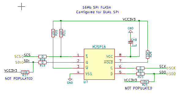
Here's the pertinent part of the spartan mini schematic, showing the connections to the SPI flash:
The spartan 6 provides a way to read configuration data from an attached SPI flash. The Xilinx Impact software is used to program the SPI flash via an indirect programming method. This all seemed pretty simple and straightforward, at least on paper. But my friend Murphy likes to show up and tell me that I can mess up even the simplest of things.
After squandering what seemed like countless hours of my life, messing around with the Impact software, I was getting nowhere. I was getting the error message "spi device not found, id check failed". That's odd I thought, I see it right there in front of me, why can't it find it? My every failed instinct seemed to take me further down the rabbit hole. I went to the schematic to see if maybe I had set the wrong mode configuration on the fpga. Then I went to check the schematic for the flash, to make sure it looked ok. I looked for clues from the manufacturer datasheet on what I was doing wrong.
Finally, when I had exhausted every last possible resource I could think of, I fished out the logic analyzer from the garage storage and clamped some probes onto the circuit :). I hooked up the probes to the chip select, data, and clock lines. To my astonishment, not a whole lot was going on. The clock was cycling a few times, but no other communication was really happening. This prompted me to start probing with the multi meter. The voice of Dave Jones echoed in my head "Thou shalt check voltages". After confirming the voltages looked ok, I started checking for continuity between the various spi pins to the fpga. It was at this step that I found that there was no continuity between the chip select pin on the flash and the fpga. Aha! Finally I was getting somewhere. Looking at the schematic I saw that there was a 0 ohm resistor(R18) in series with the chip select pin, so I checked for continuity to it, but got nothing. Thinking it may be just a bad solder joint, I was about to grab the iron to re-flow the solder, when the multi meter probe glanced off of R20, a 10k pull-up resistor, and to my surprise I got a chirp indicating that there was continuity between that and the chip select. I pulled up the board file for these 2 resistors to see what was happening.

When I selected R18 in pcbnew, the problem became obvious. The R18 and R20 reference designators were swapped. So instead of soldering in a 0 ohm resistor on R18, I had seen the misplaced reference and placed a 10K resistor in its place. Mystery solved! After switching the resistor values, I fired Impact up, and was able to save the configuration off to the spi flash without a hitch. I guess there's a few lessons I want to take away from this whole experience. First, make sure to pay extra attention when placing those references, that they're next to the right component. And second, don't wait so long to reach for the trusty logic analyzer or oscilloscope when problems arise. This may be one of the classic "trap for young players" that Dave Jones mentions on occasion.
Discussions
Become a Hackaday.io Member
Create an account to leave a comment. Already have an account? Log In.