 mosaicmerc
This approach to PCB making continues to employ toner transfer methods. The steps are as follows:
CAD DESIGN tips.
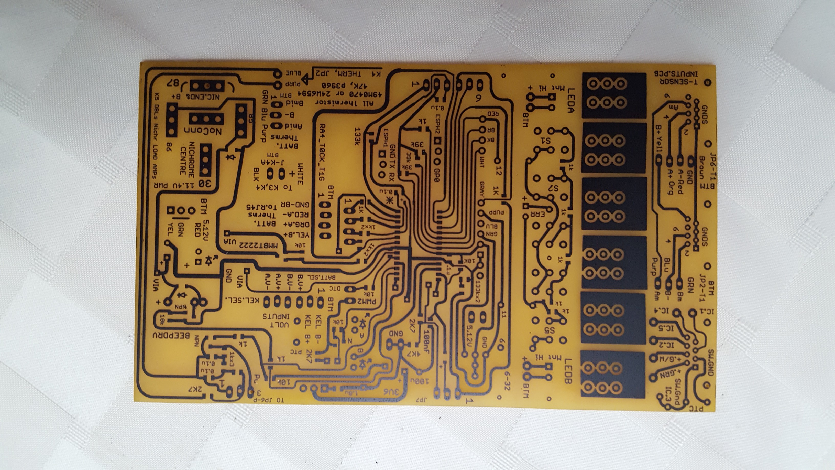
1) Design your PCB layout and add text 'silk screen' notations in the copper layer next to components if possible. I have found the EAGLE CAD vector font with 12% weight at a minimum size of .04" to .05" works well with this process. While you can add an extra toner transfer & a white foiling pass (post etching) for 'genuine' silk screening, I find it not warranted unless the PCB is single sided and you want to annotate the non copper clad side.
2) When pouring copper fills, ensure an isolation of 16 mil or more to achieve reliable toner transfer & foil transfer. 12 mil is possible but you will have to inspect and touch up with an Xacto knife for any bridging before etching.
3) Double sided boards need vias usually, I suggest upsizing the square pad to 0.031" diameter holes and .056" pad size for easy via location & assembly later. No more missed vias when soldering!
4) Locating machine screw mounting holes (6-32) requires a 0.125" drill and I suggest you add a .023" auto diameter round pad at the drill centre to mark the drill point in copper. I often use these at the PCB corners to help register/align both layers of toner transfer.
5) Always mark Pin 1 of any IC's with an asterisk in copper. Also always mark the anode of any diodes and capacitors with a '+' in copper. I also mark common SOT-23-3 transistors with a P or a N for PNP or NPN. This makes assembly much simpler as well as debugging. Note that the SPARKFUN lib has these SOT23-3 pad profiles made so that you can rout a 12 mil trace underneath an SOT23-3 transistor! That is quite helpful at times! I generally stay with 0805 SMT parts so I can rout a 12 mil trace underneath them as well. 12 mil traces can rout between 0.1" pitch thru hole parts such as IC's or headers as well.
6) Test points....most commonly I use a 2 pin, 0.1" pitch male header pad as a test point. This allows me to solder in a bare wire looped thru the PCB to make a loop on one or BOTH sides, if required, to 'hook' a 'scope probe or use DMM alligator clip.The wire loop is usually stiff wire from leaded resistor, capacitor or LED trimmings.
7) High current fills/traces: Augment high current, thick traces or fills with solder braid ...the used braid cuttings work fine, so I keep them on hand. This approach can also reduce the inductance of a trace such as a GATE drive for an FET to reduce 'ringing' or EMI issues.
8) As a manufacturing tip: I modified the standard 3 pin thru hole potentiometer pinout into a 4 hole version. The wiper then can use either of 2 holes . This permits substituting different potentiometers with different pinouts and takes advantage of manufacturer 'sales' or price breaks as often happens @ NEWARK. In the pics in this project you can find such pinouts in use. Note the 4 pin thru hole POT pinout with the connected centre holes just right of the LM317 pinout ; 1/4 width from the top right corner of this pic.-------------------------------------v
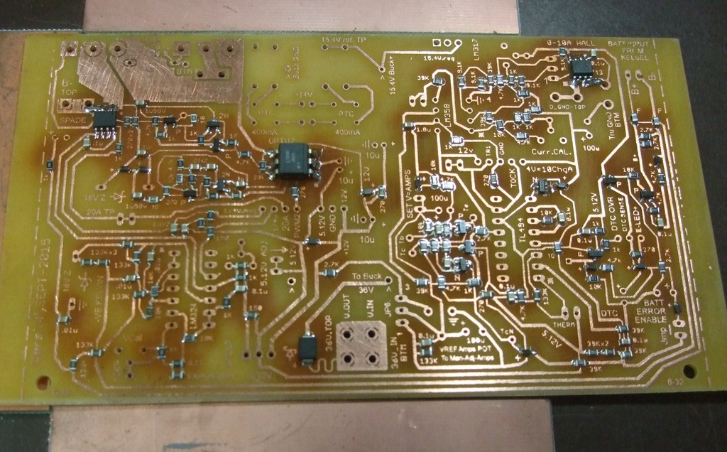
9) For double sided boards I always try to have a large ground plane fill/pour to mitigate ground resistance, ground inductance, and simply using vias to access a ground point. If you can't have a ground plane, use thick .024" or larger ground traces and star grounds if you have mixed mode analog/digital signals and switching currents to drive relays and such like. If you note the double looped 12 mil trace next to the large SMA SMT diode at the bottom of the image, that creates a free on board fusible link for any high current shorts in addition to on board PTC thermistor protection.
PCB electromagnetic compliance and electrical noise issues are outside the scope of this project but are related so here is a recent link that can assist. http://www.allaboutcircuits.com/technical-articles/clean-power-for-every-ic-part-1-understanding-bypass-capacitors/
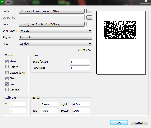
See the Build instructions below the pics = making PCBs.


 chris.coulston
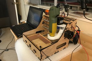
 Timo Birnschein
 Chromico
 tonyo
tonyo
Yes, I hear brother Toner is fused at a higher temp. I use a sanding stone block (hardware item for prepping cement plastered concrete walls before painting) to deburr edges occasionally but it's not really req'd often with the diamond cutting disc I use. Thanks for the observations!