 David Scholten
So first of all, all of the design files have been uploaded (well, the newest versions anyway) and are available for download. The original intention of this project was to make a nifty little product and sell them on eBay. However, due to some bad economic decisions with the component selections, I can't see the grid-2-audio unit being profitable in small batch production. As a result (and to Hackaday's liking) I'll just upload all of the design files here for anyone with a non-commercialisation intent.
Summary of 1.0-->2.0 PCB changes:
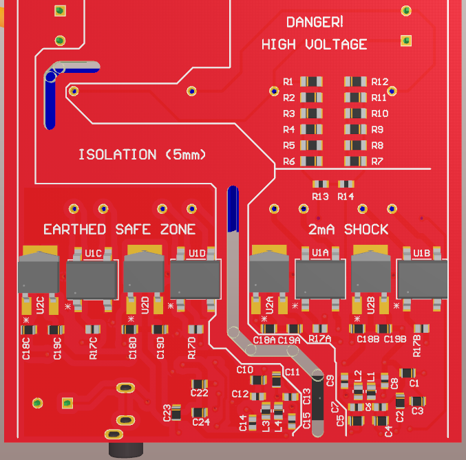
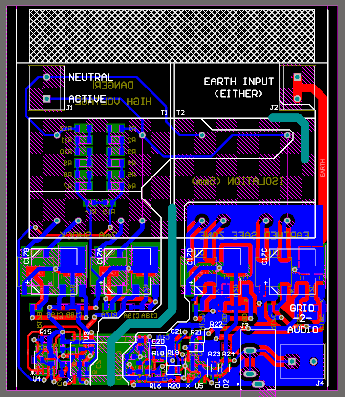
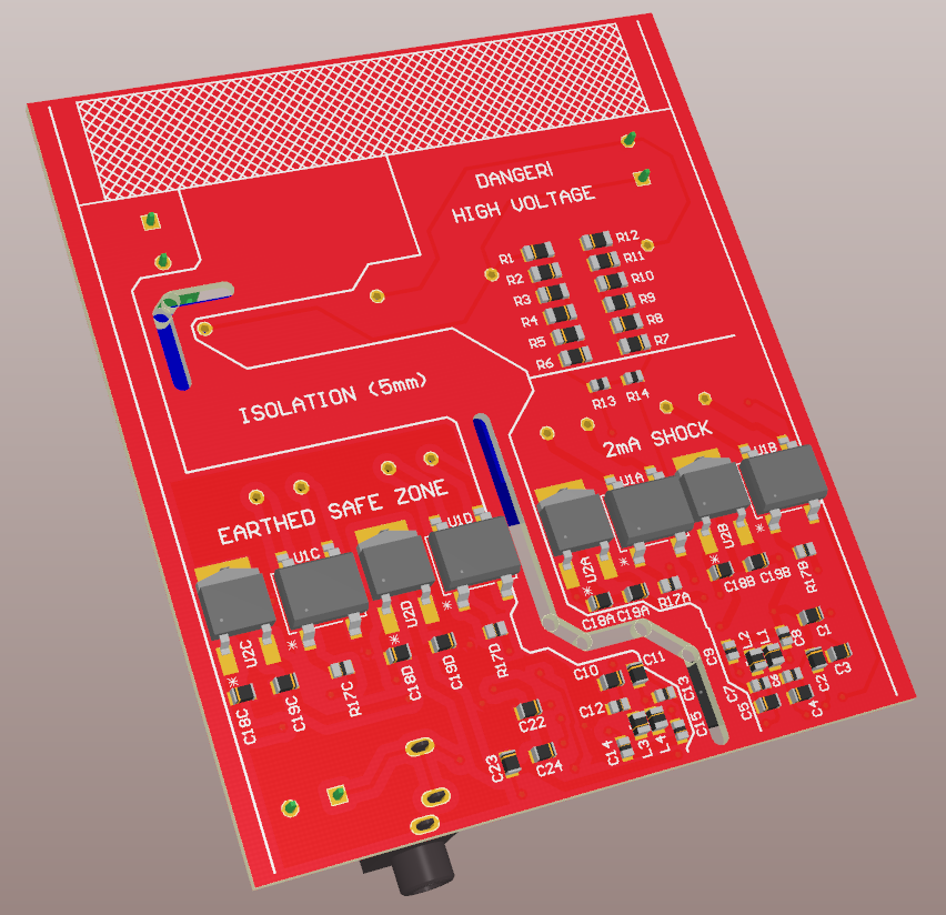
Number 1: Safety! The obvious safety concerns were the clearance from the mains potential to earth and the short-circuit shock capability of the mains measurement circuit should it be touched/connected.
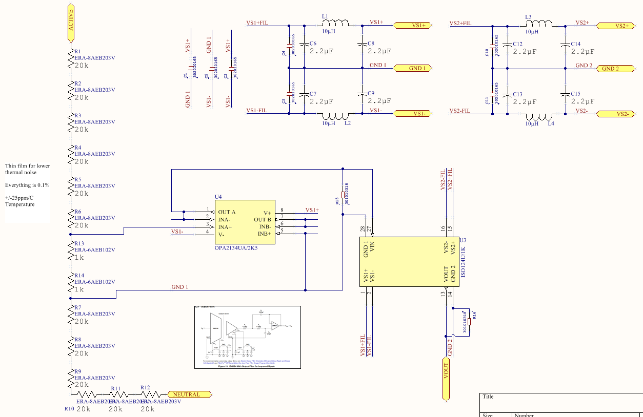
-->There are two dangerous regions: The mains active/neutral region (lethal) and the signal processing region that is referenced to the mains (current limited during shocks). The voltage divider across the mains has been increased from 60kOhms to 240kOhms. Based on the arrangements the practical shock hazard of this region has now dropped from a ~7-8mA shock to a ~2mA shock. This is no longer dangerous even if a person were to experience it (it still hurts). Increasing the resistance of the mains voltage divider sounds like it would introduce noise, however this is not the case as the actual voltage difference is measured across 2kOhms. The divider acts like a 2kOhms in parallel with 240kOhms to the following op amp and so any noise is effectively dampened. However, that 2kOhm resistance is at the limit of what the opa2134 op amp can tolerate before another circuit is recommended by the datasheet (not to mention the op amp’s input capacitance starts to affect the upper frequency bands at 2kOhm).
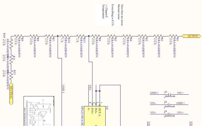
-->The minimum clearance between the earthed section of the circuit and the hazardous regions of the design was increased from 2mm to 5mm. This certainly is clearance enough from the "2mA shock" region, but I also added some 2mm cutouts in a region where the active connection comes within 7mm of the safety earth. Cutouts were also added throughout most of the isolation region just for the sake of good practice to maximise the creepage distance where ever possible:
Number 2: Footprints…
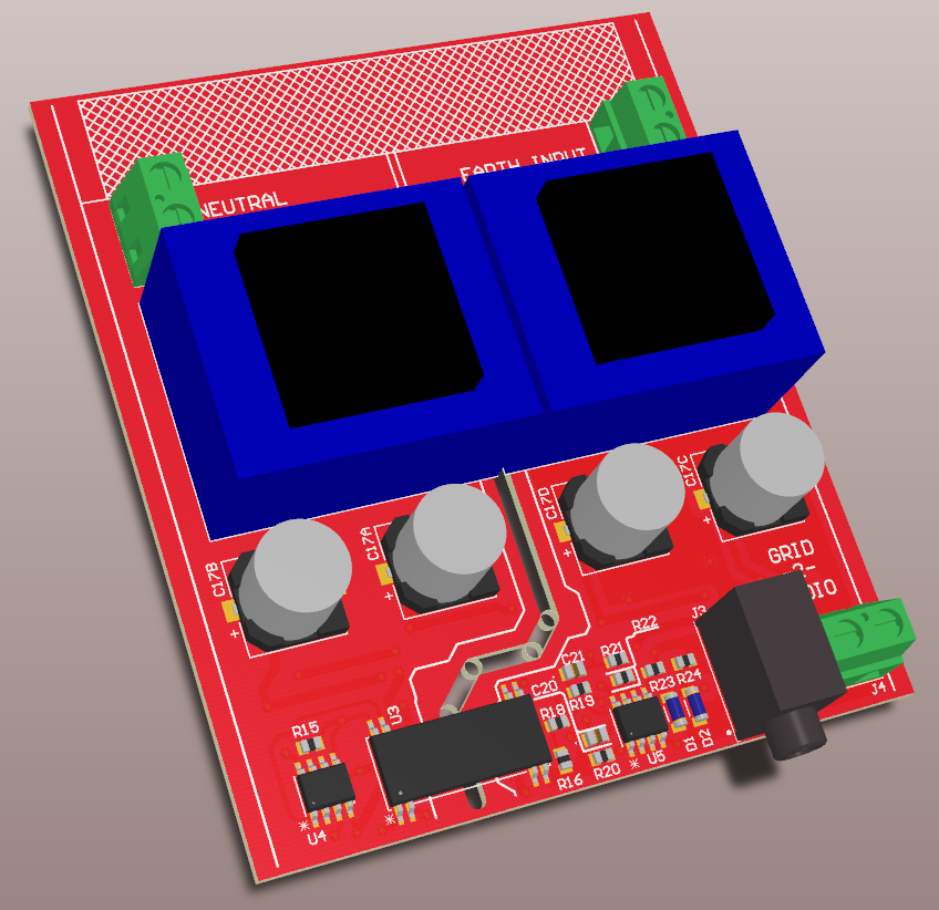
-->The 3.5mm headphone jack footprint that I downloaded did NOT have slotted cutouts! Although the 3D model did and the footprint pads were elliptical, I missed this completely. This has since been corrected.
-->Fixed all of the 100nF bypass cap issues with gerber viewers. Although the final V1.0 PCB turned out okay, the manufacturer’s gerber viewer wouldn’t display the 100nF pads at all (only the top solder cutout for the pad). I simply went into the footprint and deleted/recreated every piece of geometry and it fixed the problem?!?
Number 3: Stupid mistake.
-->This is a good one. I connected ground of the 3.5mm audio jack to the output signal and vice-versa. I’m glad I caught this because it’s the kind of mistake you can live with (using an adaptor cable) and be reminded about constantly for the rest of your life.
->
-->
--->
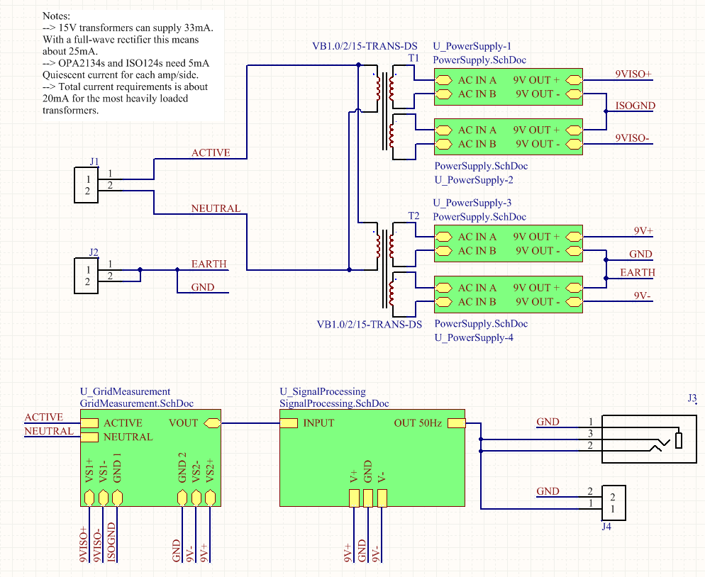
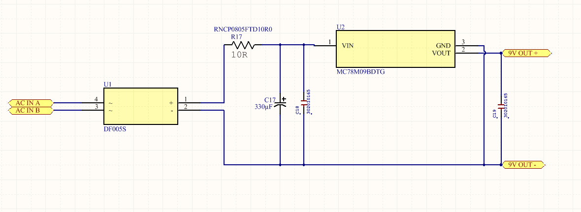
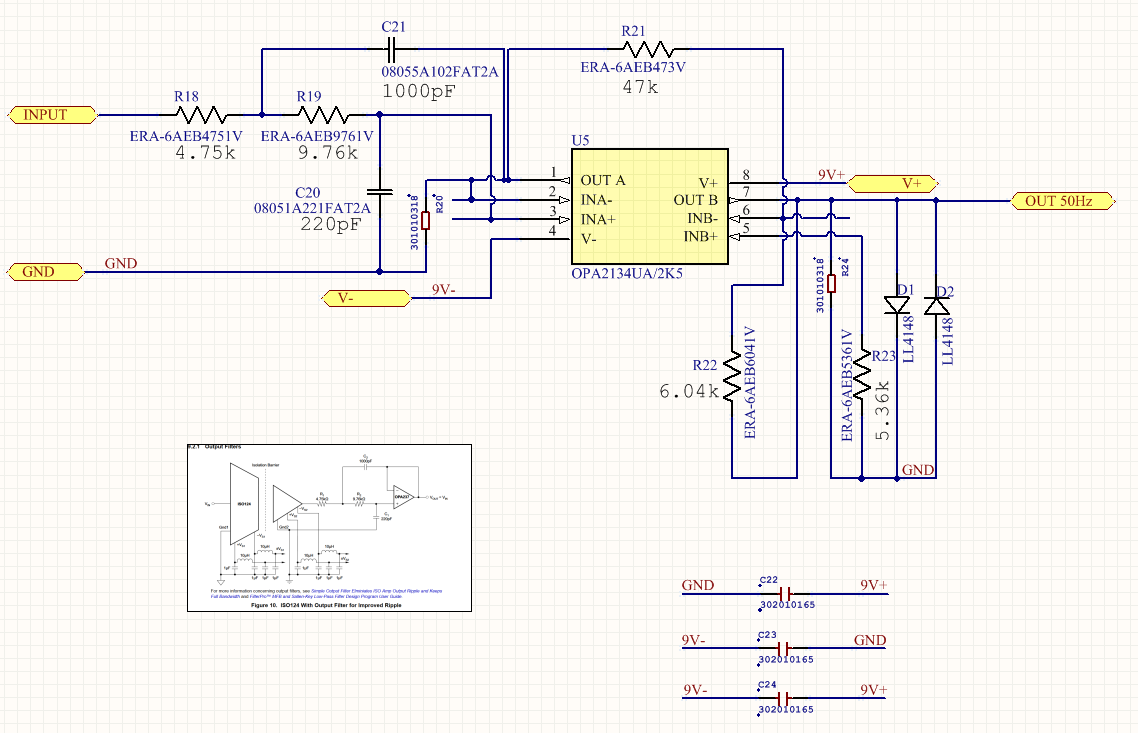
Right, now with that out of the way I present the “final” schematics/layout pictures, which are ALL available in the project files directory in Altium form:
Discussions
Become a Hackaday.io Member
Create an account to leave a comment. Already have an account? Log In.