 Yann Guidon / YGDES
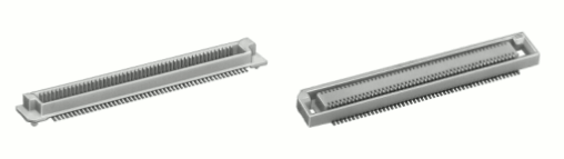
The final design will use the 100-pins Hirose FX8-100 connector. The PDF contains these pictures, to give you a rough idea :
The stacking height is only 3mm between two boards. Actually it will vary because the PCB wil bend ;) but pairs of PCB can be easily mated and moved up/down the stack as needed, that's important for modularity and repairs.
Why this connector in particular ? Well, in another life I was a ETX PC/COM format enthusiast and by chance I got a half-reel of FX8-100S-SV from eBay (this can happen why you buy a box with "various parts" that the seller has no idea what they are or why they are useful and can't list what they sell... you're never safe from a good surprise !)
Since this connector is used for the ETX COM format, availability is rather good. It has a lot of pins and the stacking height is about the thickness of SMD parts such as SOIC ICs.
Now let's see the little issues :
- The pin pitch is .6mm, it's not extremely thin, but thin enough to prevent wires from crossing from one end to the other with a standard 150µ etching rule. 150µ wire width and spacing is ok to run 2 wires in .6mm but there is no room left for the vias. The approach today is simple : use 2 contacts for one signal, so only 50 signals are available. This increases the number of required connectors... Maybe 3 or 4 are necessary.
- I only have S-type connectors (a few hundreds). The complementary P-type is harder to get. I'll be investigating in the coming months, to find decent prices (sub-$) in medium volume. It seems that compatible connectors are made by another manufacturer, that could be a clue...
When I have enough male/female pairs, I'll start designing a support board and generic flexible "pages" :-)
Discussions
Become a Hackaday.io Member
Create an account to leave a comment. Already have an account? Log In.
Last time I look, I think 0.8mm is the finest pitch dual row connectors that was usable. My Chinese proto PCB place uses similar design rules as yours (except for the size limits).
Are you sure? yes | no
These FX8 connectors are surface mounted so I'll simply make 0.3mm wide traces that connect opposite pins... why make it more complex ? :-)
If I chose to connect the male and female connectors directly on top of each other, the "key" bump will make it impossible (the circuit is too thin), the mechanical rigidity will be too low, and it's still impossible to route wires from one edge to the other (unless they are routed around the connector but then, the trace length increases.
I would either need 0.8mm pin pitch or 100µ design rule...
Are you sure? yes | no
From the picture, it looks like you could breakout and drop vias for every other pin inside the footprint. If all else fails, consider using those inaccessible pins for ground connections and that should give you good signal integrity across PCB.
Are you sure? yes | no
My fab is limited to 150µ rules and however I turn it, vias create more problems than they solve. I'll add ground vias here and there but probably every 5 positions or more.
One via is 300µ drill surrounded by 2×150µ ring, that's .6mm on both sides of the board. It's possible to have a via for every pin, by shifting odd and even vias. This leaves 600µ maximum, or 2×150=300µ if we remove the spacing with the via. 300µ is not enough to route 2 wires 150µ each...
Fortunately the #Discrete YASEP design is pretty resilient and doesn't work extremely fast. The stackable bus system I'm creating has a pretty high fanout but I managed to keep lengths reasonable, it should not exceed 1 foot. I don't know if I'll have to add terminations (clamps ?) at each end, it will vary too much from pin to pin...
You will see when I make the first prototype ;-)
Are you sure? yes | no