 Yann Guidon / YGDES
The first description of the first board gave the intended functions (data entry and display) but suffers from several problems. The most obvious is that it is too complex and it stems, I found, from mixing data input with display.
When these functions are separated, things become easier and clearer. So we'll have a second board ("page 1A") on the left, that is dedicated to data entry, and the data display ("page 1B") is on the right.
The display system is considerably simplified. It's just a matrix display, the inputs are constantly scanned, byte per byte, 8 bits are translated to 2x7 segments during each cycle and there is no button to make it more complex.
The matrix approach reduces the current in the LEDs so they draw less power. Further power saving is possible by turning off the digits that display leading 0s. The required logic is manageable, though I might have to use some basic programmable logic here and there, to keep cost and complexity low. SOIC versions of 74HC families are often more expensive than some tiny FPGAs or a PIC...
The other cool consequence of this better, split structure is that the scan of the bus can also be used to send data for remote monitoring. There is an internal bus of 8 bits that gets consecutive values from here and there, these values can be sent to a UART (or USB converter).
The "Page 1B" display is made of 3 parts :
- the input bus latch&scan logic, that selects consecutive bytes
- the UART that receives the stream of bytes from the bus and serialises them to the host computer
- the matrix control that converts to 7 segments, removes leading 0s and drives the columns and lines.
.
Those parts can work with the same clock, possibly a UART clock. Delays between scans can be inserted to reduce the display luminosity. 500 to 1000 scans per second are desired to avoid visual fatigue and keep the host computer up to date of the processor state.
To increase the turn-on ratio of the LEDs, bytes from the scan bus are grouped into 16-bits words to provide a 1/8 duty cycle instead of 1/16. Only two 7-segment decoding chips are needed. This makes the leading zero detection a bit simpler too. 74HC573 are cheap when sourced by the 1000s.
Serial output
With a 115200bps serial rate, the interface can send 11520 bytes per second (1 start, 8 data, 1 stop). When transmitting 16-bytes packets, 720 packets can be sent every second.
115200Hz is obtained with a 1.8432MHz oscillator divided by 2^4=16. Since we also need to scan the keys and LEDs, a further ÷16 counter/divider is required. This is the perfect job for a CD4060.
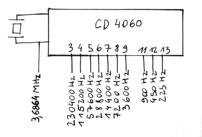
We have overlooked the start and stop bits. At the same time, I have a whole lot of 3.6864MHz crystals. A 74HC165D shift register can load the byte from the bus and serialise it to the output at the desired frequency, to emulate a UART. But the CD4060's missing "Output n°10" is sorely missing, a CD4040 comes to the rescue.
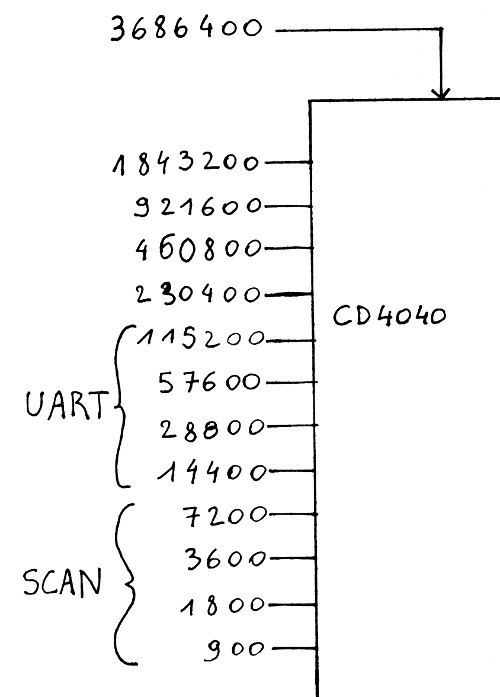
The CD4040 doesn't have an integrated crystal oscillator but it fits perfectly. From out point of view, it provides two cascaded 4-bits counters that we use in several parts on this "page".
The slowest counter/nibble provides 4 wires to scan the keyboard and the bus, 900 times per second.
The 16 bytes need 7200 bytes per second. This is multiplied by 16 again and sent to a shift register, so we can send bytes faster than they are scanned from the input bus :

The circuit has not been tested but this is how it should work :
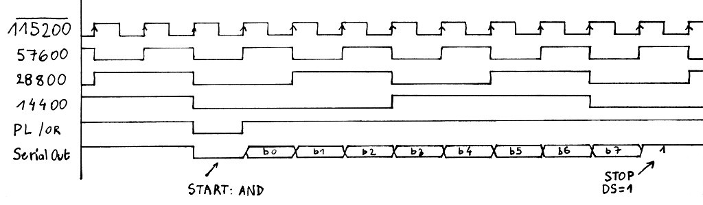
(Correction : the 7200 should be ANDed too, no ?)
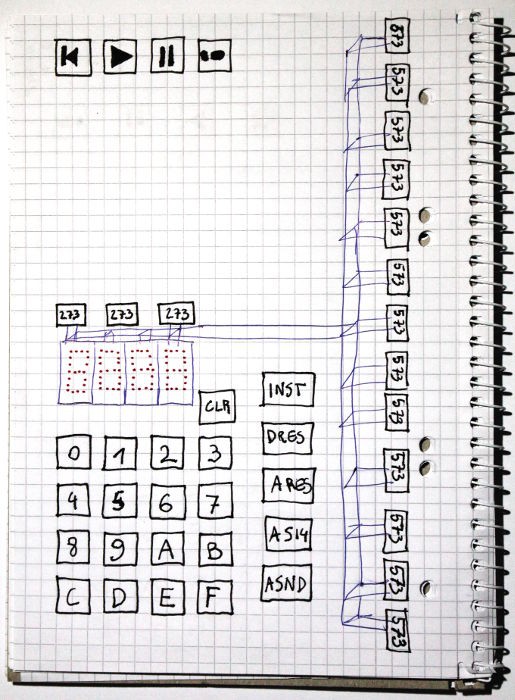
The data entry "page" is split into 4 parts :
- UART
- keypad
- FIFO
- Bus buffer/driver
The UART can also receive commands from the host. Those commands should be in the same format as the user's input on the keypad, to keep the complexity low.
Thus the rest of the input logic can receive byte streams that must be interpreted, the source is not differentiated - the commands are simply ORed.
Some commands are "data" commands : the input of a hex digit. The data nibble is sent to a sort of FIFO of 4 nibbles, to queue the values (MSB first).
The other commands trigger a "transfer" of the FIFO's contents to another register and/or the bus output, which can trigger bus activity.
Side effects and commands will also include a FIFO clear and a serial dump during the next display scan cycle. Pointer auto-increment should be handled too... I keep some free room for later.
Command format
The host sends commands as a stream of individual bytes (which is perfect for a serial port). The "data" and "action" commands are made of two nibbles. The lower nibble is actual data (the hex nibble sent to the FIFO, or the number of the register to write).
| low nibble | high nibble | |
| Data packet | hex data | 0x1 |
| Command | Reg. number | 0x2 |
Higher bits might be used as "options" for the commands, such as enabling auto-inc of pointers, I have "reserved" the remaining MSB for now.
A host computer will control the system by sending a stream of 0x1? and 0x2? bytes. For example, to load the value 0xABCD in the regiser R2:
12 ; register 2
22 ; write FIFO to ARES
1A ; fill the FIFO with ABCD
1B
1C
1D
23 ; write FIFO to DRES
This sequence of bytes is the same as a user would type on the board. See below "User Interface".Keypad
The keyboard scan logic shares some signals with the display's logic and work at the same speed to avoid redundancy. I have not figured out everything yet...
User Interface
The new system saves the press of the "valid" key so it is a bit more convenient as well. The order of the commands is a bit modified though :
- Input 1 to 4 hex digits on the keypad
- Press one of the command keys to send the data from the FIFO to the specified bus.
To read a normal register:
- Input the register's address on the keypad (1 digit)
- Press the ASI4 or ASND key
- The value appears on the corresponding LED display on page 1B.
To write a value to a register:
- Input the destination register's address on the keypad (1 digit)
- Press the ARES key
- Input the register's new value on the keypad (1 to 4 digits)
- Press the DRES key
(both values should be displayed on page 1B)
Discussions
Become a Hackaday.io Member
Create an account to leave a comment. Already have an account? Log In.