 Yann Guidon / YGDES
Page 1A has a sort of FIFO, actually a shift register, that I'm happy I solved with a reduced component count :-)
The FIFO accepts 4 input bits and queues them until another command latches them in a different buffer on the main bus.
The input nibble (that comes from the keypad or the UART) is latched by the lower half of a 74HC273. The higher half's input comes from the lower half. This is chained further into a second '273.
Each latched nibble is sent to an individual TIL311 hexadecimal display. It's a bit expensive but
- it does not need external parts (ie for decoding)
- only 4 are needed
- it adds a classy retro touch
- I got a nice deal on eBay
- the digits are pretty, clear and look cool !
The "not-7-segment-y" look won my heart. However these modules draw quite some power (it's vintage 1972 technology, 60mA for the decoding logic plus as much for the LEDs !) and some logic is required to disable leading 0s. A 5-inputs OR and a 3rd '273 should do the trick. The three '273 will get cleared (low pulse) when a command is sent (tbd).
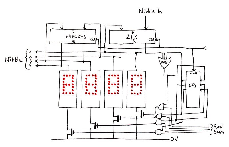
More power might be saved, maybe by synching the digits' output enables with the keyboard scan, so only one TIL311 is turned on at a time. Cost : 4 AND2.
I have not found a use for the 2 decimal points so far.
Except for the TIL311, all parts are fixed-function, surface-mounted, low-profile and low power, so the design goals are reached for this part.
Discussions
Become a Hackaday.io Member
Create an account to leave a comment. Already have an account? Log In.