 Yann Guidon / YGDES
At this point, I "can" (read: know how I could) send data from the P1B board to a USB-serial dongle with relatively few gates. Now I must find how to do the reverse to receive data on P1A.
Flashback
I still remember building a UART board as one of my first PCBs, around 1991, as an unexperienced teen. I used a AY-3-1015D integrated UART (DIP40) found at RadioShack. It never worked but "I learnt a few things" along the way.
Other hackers have followed this route before, one of the last being @matseng
But as I understand it, his receive system uses an "analog hack" that is too delicate to calibrate.
Back to 20151022
I got the clock and I got tens of 74HC595. I could even make a shift register with a 74HC574 or 74HC293. I have also already written 2 working serial receive circuits in VHDL so it shouldn't be hard to design another with TTL-style logic. But for this project I don't have the luxury of spawning arbitrary logic with a few key presses and some clicks.
The shift register is only the easy part of the story. Serial reception is classically the domain of finite state machines, with counters peppered here and there. Furthermore, that kind of circuit has to work with several clock granularities because
- If you have an existing clock at the right baud rate, it doesn't matter because the sender certainly is phase-shifted. We can forget the baud generator of board P1B.
- You need a main clock that is a multiple of the baud rate (we got it already)
- You have to divide this clock again to get the baud rate, but you have to synchronise it "somehow", so it runs with the right phase.
- Oh and once synchronised, actual data synchronisation happens by delaying the shift clock by half a bit-time, not a full bit time, so you have to handle two durations...
Let's add another constraint. No, I don't care about parity (we're doing 1 start and 1 stop bit only). To increase reliability, the start bit must be low during a whole half cycle. Only then can we start shifting data in.
In my VHDL designs, I reduce the complexity and save a few gates with a little neat trick : the shift register is reset to all 1s before shifting the start bit in. When the last bit of the shift register is reaching "0" we know that all the data bits are shifted in. Then we just have to check the value of the stop bit, if it reads as "1" then the byte is valid.
With the '595 or the '273, the CLR pin clears the registers to 0. This inverts the whole logic but it is still possible : just OR the data input pin at the right moment, to make the start bit look like 1. The shift will end when the last bit (at the other end of the shift register) changes from 0 to 1.
The choice of the part will depend on whether I'll need the '595's tristate output.
The "shift trick" is useful in VHDL because I want to keep the gate count as low as possible. However I can instantiate as many bits in the shift register but I can't hold the necessary 9 bits in the '595 or the '273.
With this discrete system, I might as well use another CD4040 with its extra divider stages and they can be used as a substitute for a proper finite state machine.
In fact, this counter also looks like the digital analog to the ramp in @matseng's design. If we tap and combine the right signals, it becomes possible to sequence the right pulses at the right times, and its digital nature makes it immune to later baud rate modifications.
My VHDL code normally handles a few transitions (hence states)
- Idle/waiting
-> if the data input is low,
-----> the baud counter is initialised to half a bit period and goto state 2 - START bit validation : decrement the baud counter
-> if data input is 1 then return to state 1
else
-----> if counter expired then init baud counter to bit time and goto state 3 - SHIFT state : decrement the baud counter
-> if counter expired then
-----> if shift register is full,
---------> check the value of the stop bit, buffer the register's data and goto 1.
-----> else
---------> shift another bit in the shift register and init baud counter to bit time
This is a 3-states machine with 1 count-down baud counter and minimal random logic. Maybe I can come up with something else using a CD4040 ? Let's see...
The '595 and the '273 latch on a rising clock edge. If we look at the right output stage of the CD4040, this corresponds to the half time of a bit period (and if not, we can still complement the clock bit).
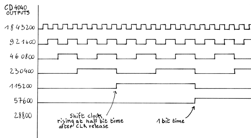
Another "trick" for the START bit detection : we can use the serial data input to control the counter's reset line (after a NOT because CLR is active low). This starts the counter from 0 when a falling edge appears. After a while, one of the outputs (here, the 115200) goes high and we can use this information to say "we got a long enough low pulse".
So we have detected the start pulse but the rest is possible only if we can keep the CLR input from going low again, at least not until we have shifted everything in. A feedback gate is necesary.
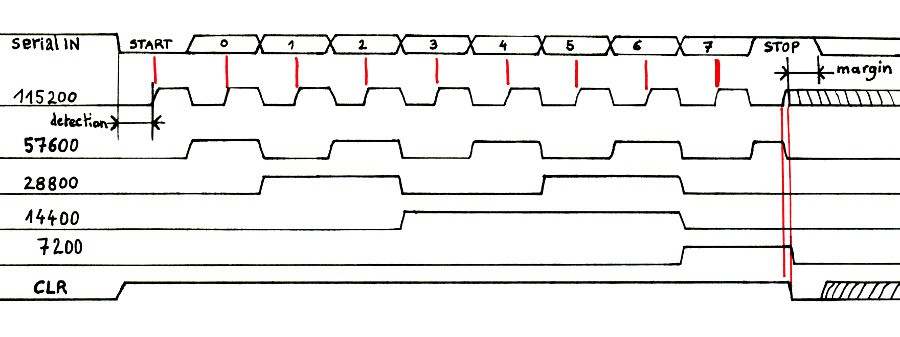
The final circuit doesn't implement the "short START bit detection" because it is too unlikely to happen. Instaed I have built the control circuit around a synchronous RS structure where reset has priority over set. The delay that the DFF gate adds keeps the output signals clean with fixed 300ns transients/pulses at the output of the AND3 gate, which can trigger other circuits.
The principle is simple :
- Set CLR high when Din is low
- If 115200, 57600 and 7200 are high, pull CLR low and send a strobe to V (if Din is set).
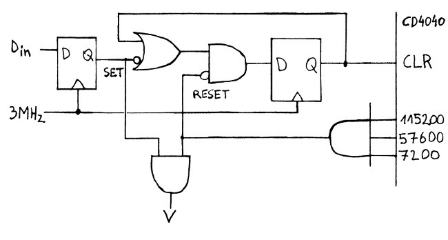
This design is not the best but it's simple, cheap, works "in nominal conditions" and uses only available simple gates.
- binary counter : CD4040 or similar
- shift register (not represented) can be a '595, '574 or '273...
- 2 DFF (one 74HC74 ?)
- 4 AND2 (one 74HC08 ?)
- 2 inverters as used for the Xtal osc: NC7ST04
- one OR gate (can be a SN74LVC1G type)
The SET/RESET logic (OR-AND) can be reduced to a single 3input gate, such as some modern SOT23 gates.
The circuit does not reset if short pulses are present but the input DFF resamples Din to protect against very short transients. It's a good compromise.
Found at http://digitarworld.uw.hu/circuits.html:

Discussions
Become a Hackaday.io Member
Create an account to leave a comment. Already have an account? Log In.
Cool, looks like there'll be a discrete UART design for me to plagarise when the time comes :)
Are you sure? yes | no
I'd be very curious to see your "rip off" ;-)
However I believe you should use a different design, inspired by my VHDL version instead, because we have different sets of constraints.
If you can have "reset to 1" DFF gates, then the "shift register trick" better for you. That would be 9 or 10 DFF1 for the shift register, the last in the chain being the "finished" flag when it goes to 0 (as it outputs the start bit). You could use ×8 oversampling to reduce the number of Div2 gates, with a lower main clock frequency that is an exact multiple of the serial speed (in my VHDL design I divide a non-multiple, higher frequency like 50MHz so the counter design is more complex).
Maybe I could help you design the serial receive unit, if you haven't done it yet. You'll need DFF gates that reset to 1 and 0 though. I'll see what I can do...
Are you sure? yes | no