 Yann Guidon / YGDES
After more work, here is the circuit diagram for the SHL unit!
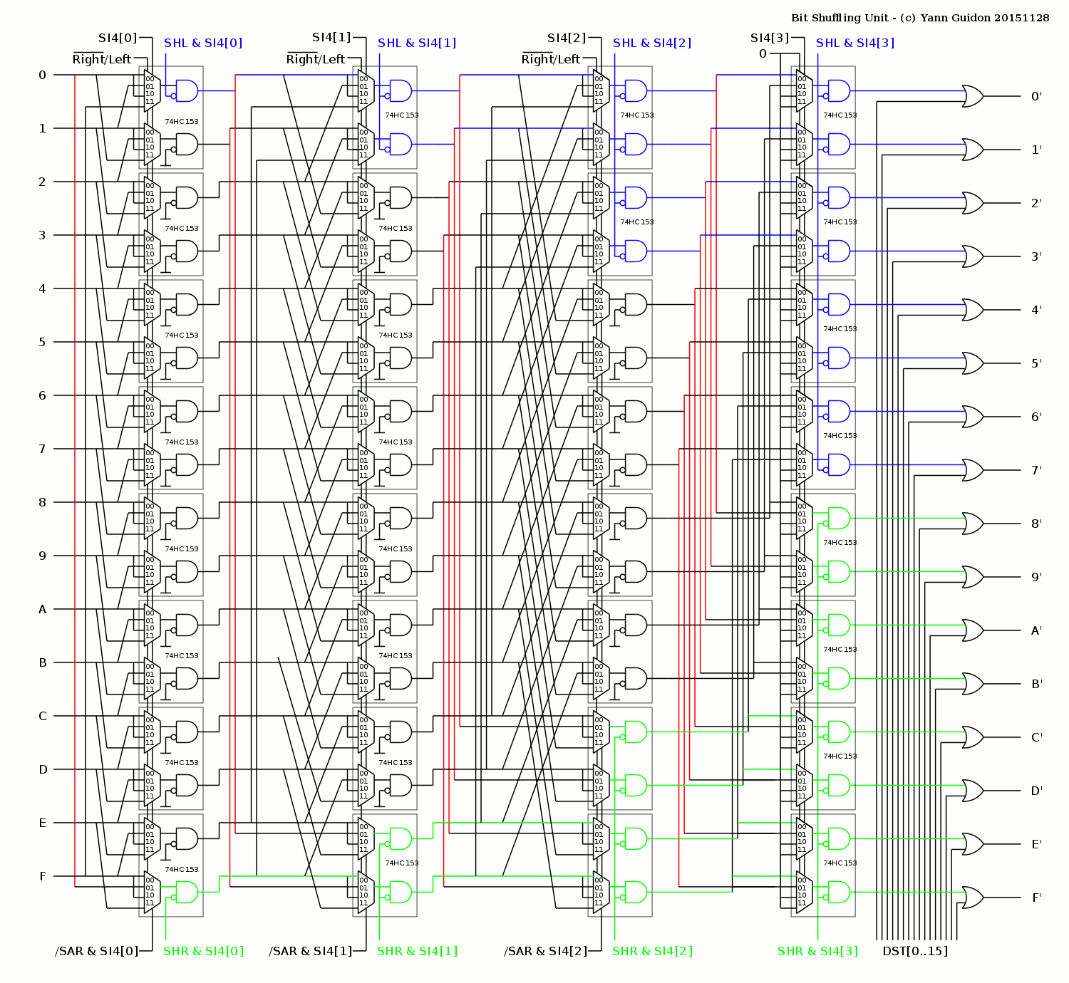
I have tried to make the function a bit more apparent by using some colors.
One cool detail is that the last stage is just a "swap" layer, made of MUX2. However, it is more interesting to keep the '153 because it contains 2 AND gates so if a '157 was used, a half 74HC08 would be needed.
Here, some inputs are wasted but the circuit's structure remains very regular. The unused inputs might also be used to extend the functionality of the unit, with finer insert/extract operations.
The chip count is 32×74HC153 (dual MUX4 with enable), 4×74HC32 OR gates and some more logic for the control. Some more '08 might be needed to mask some bytes of the DST operand.
The critical datapath is 5 circuits, which is pretty good for such a versatile circuit. Indeed, it can also perform the operations of the IE (Insert/Extract) unit that manages/aligns bytes from/to memory (more control logic is required though).
Many AND inputs are tied to 0V. This could instead be tied to a global "enable" signal that reduces signal swings in the unit and save some power.
I think that this unit is very cool, despite its significant size. Though it would be worse with transistors ;-)
Discussions
Become a Hackaday.io Member
Create an account to leave a comment. Already have an account? Log In.
May be you can reduce the layers by looking into much wider input multiplexors.
74HC4051: 8 to 1 mux
74HC4067: 16 to 1 mux
So just have to use 16 of the HC4067 to make a barrel shifter in a single layer. Also you can reduce the fan-in by breaking a larger shift into 2 or more cycles.
Are you sure? yes | no
That's an interesting thought and also another example of finding the best compromises. But first, https://en.wikipedia.org/wiki/List_of_7400_series_integrated_circuits says:
"744067: 16-channel analog multiplexer/demultiplexer"
It's not suitable because the signal will be weaker at the output (been there, yada yada). These chips don't draw much power but usually have tens or hundreds of Ohms of resistance which requires further amplification if you want to run fast enough. I'm picky here but... it's still an argument: let's not mix analog and logic gates ;-)
The MUX8 gates are interesting though. The 74HC151 is used here and there but in the SHL unit, it doesn't save anything because it would replace only two layers (remember, the bits go left and right) with only one chip per bit. The '153 uses one chip for two bits for one layer, so there are still 32 MUX chips.
Reducing the number of layers is not critical anyway. The control logic is still "simple" and some little headroom remains at the last layer for more functionality. The slowest circuit in the "operation" critical datapath is the 90ns Flash that contains the multiply tables.
One interesting thing however is to use as many chips of the same reference because this helps buy cheaper in bulkier orders. The '153 and '253 (same but with tristate output) are used a lot, it appears, so let's reuse them as much as possible :-)
BTW, using wider MUX doesn't necessarily speed thing up: the fanout in the above circuit is a constant 4 but with a MUX8, it becomes 8, which slows things down a bit. With the '153, the fanout is reasonable and there is this tiny killer feature : the integrated AND helps reduce the chip count (and speeds things up because it's integrated so there is almost no transmission delay).
OK I just checked : the '151 has an /enable pin. But the original idea with MUX2s didn't have this luxury :-)
Are you sure? yes | no
The 16:1 mux has resistance of 70-160 ohms. It is not too bad for a single stage as you'll buffer the outputs back into the register anyway. Since you are not running at tens of MHz, it shouldn't be too bad. The input capacitance for a single layer is going to be more an issue as you have fanouts of 16 MUX to feed.
I suggested splitting the shifts so you can get by with fewer stages. There is not a lot of speed ups for single cycle shifts as you don't exactly do back to back shifts. :)
PCB real estates can get expensive at some point for prototyping - much faster than chip cost.
Are you sure? yes | no
I wouldn't use an analog MUX16 anyway because, despite almost immediate propagation of the input, the control path/decoder is not optimised for switching speed. I'd like to keep the SHL propagation under 80ns so that's a budget of 20ns per layer (max, without the control logic). Now if we take a worst case resistance of 200 Ohms and 16×10pF load, that's 32ns through only one layer. That's ok for one half of the propagation delay but it's impossible to use as is without amplification because the 2nd layer will add another resistance and even more load in series... The signal at the outputs will rise much more slowly.
I'm not interested in splitting shifts because... I can do it in one cycle so why make it slower or more complex ? And I often work on code (like crypto, graphics, simulations or compression such as #Recursive Range Reduction (3R) HW&SW CODEC) that does tons of bitfields insertion/extractions. I have often cursed lazy CPU designers who half-built their shifter unit... Rotation can be life saving, and the YASEP has an optional OR-combine to save one instruction in some critical code ;-)
Oh and PCB real estate is a very conscious choice. The final system is expected to span half a square meter anyway :-P
Are you sure? yes | no
Your bare PCB budget alone is much larger than my entire FPGA board. I had to squeeze very hard to fit everything I want inside a 10cmx 10cm PCB deal. :P
I was hoping that the shifter could be done in single layer. If only there are digital mux, then wouldn't need to worry about buffering.
Are you sure? yes | no
I know the printed circuit surface is going to cost a lot but that would go down if some tens of units are manufactured in a suitable factory. Prototyping will be expensive but I would do otherwise if I wanted it differently (I have enough FPGA boards to play with) :-D
Your FPGA board has a totally different purpose and we use different means. I see the #Discrete YASEP more like a sculpture (like the #The T-1: A discrete 8-bit Stack Computer), an engineering statement, than a really functional computer for professional use.
Yet, there are compromises to do. The purpose is to be totally observable and understandable, totally self-contained, and between chip cost and surface cost, the choice is easy: the more surface, the easier it is to understand/examine the whole thing. I could fit the YASEP in minuscule FPGAs but this would bring nothing, it would only add obscurity and mystery...
Are you sure? yes | no