Yann Guidon / YGDES
-
What about the sound ?
01/08/2016 at 13:09 • 2 commentsOK I forgot this : a 16-bits mono sound output should be easy to create.
A nice FIFO (4K words ?), a good 16-bits DAC, a configurable clock reference and we're done, right ?...
Oh, I might have found cheap ADCs (8 bits, unipolar, 200Ksps). Should I ?...
BTW the YASEP architecture has some features that are inspired by DSP but it's not the computational aspect. Yet is would be FUN to do some real-time sound processing "for educational purpose" :-)
For the "FIFO" I could reuse the IDT7132 dual-port SRAM (2K×8). The counters would be "discrete" and easy to read back. The free-running output counter is a simple 74HC4040, whose value can be exposed in a Special Register and current queue depth can be computed in SW. Sound data is sent to another SR, which increments another counter (easy to read back too). A 4th SR configures the frequency, start/stop etc.
2 channels of input and 2 channels of output, all 8 bits, sounds like a plan. Now if only I could get a reasonable, meaningful sampling frequency out of the 3.6864MHz oscillator ? It sure won't work with 48KHz or 44.1KHz systems.
- 3686400/225=> 16384Hz (this could be increased to 32768 by detecting both edges of the clock)
I consider using a faster main frequency generator, which will enable finer control signals sequencing, maybe 18.432MHz or 24.576MHz. The choice also depends on the ability to easily derive standard serial data rates:
- 18432000/48000 = 384
- 18432000/115200 = 160
- 24576000/48000 = 512
- 24576000/115200 = 213.333
18432000Hz seems to be the winner so far, though it brings only 54ns of resolution for scheduling, instead of 40.7ns@24.576.
Obviously I want to keep a single clock source and derive all the others (serial, sound) to keep the design as synchronous as possible. I don't want to have to deal with Gray codes or multiple clock domains.
A variable sampling clock can be created by feeding the 18.432MHz frequency to a 74HC4040. A 74HC688 compares the output with a value loaded in a 74HC574, and triggers a /RESET of the 4040. Minimum sampling rate would be 7200Hz (minus the off-by-one).
Feedback is welcome !
Why do I even bother about a FIFO for the output ?
A simpler approach is : just map the output buffer in one of the data RAM spaces. Create a shadow SRAM that gets written just like the other banks, addressed by the corresponding Ax register.
This saves instructions and increases speed, since a normal operation can write to the sound output. No need to execute a PUT instruction.
This also saves circuits and complexity : there is no FIFO write register to GET, you can AND the Ax register to perform circular buffering. You still have to GET the read pointer though. But this saves the 74HC4040 for the write pointer.
Something similar might be possible for the ADC input but it's hard to write to both SRAM banks at the same time. I must find another trick...
-
Thinking about a framebuffer...
01/08/2016 at 12:54 • 3 commentsI would LOVE to provide a decent video output to this system. However modern displays easily exceed the capacity of a 16-bits CPU.
I don't want to limit the display to 320×200px like the mode13h in the ol'PC. I'd like 800×600 or even a decent 1024×768×24bpp. I don't mind if it will be slow :D
There are 800×480 LCD modules with cool prices, which is good for text and pictures display. A 16-bitter could work in R5G6B5 color space for faster updates. And I'm OK with breaking the "TTL rules" and use a FPGA instead of slow HC parts. After all it's just counters and latches and...
No, the real challenge is how to let a 16-bits CPU access a much larger addressing space. In the case of a framebuffer, this might be easier conceptually because the display is 2-dimensional and I have chosen to use 2 different registers to address a single pixel.
This means : a couple of new, special purpose instructions to set and get a pixel value.
pixget rX rY rdest
pixset rX rY rCol
pixset rX rY imCol
The architecture allows 3 register reads per instruction and we can even get a 16-bits immediate version :)
This also saves the user from having to deal with horizontal and vertical resolution. Coordinates will just be clipped, to 10 or 11 lower bits.
Wait.
11 bits means 2K pixels per dimension, or 4M pixels, or 8MBytes. Where will I find that and how will I manage that ?
Internally, there would be a 2K×2K virtual display area and only some of it is scanned to send to the display. The CPU can "scroll" by changing the start address, both X and Y (I told you, it's just counters...).
If I select a 1K×1K resolution, that's nice for a 800×480px display but the scrolling is limited... I hope to make some little games so hardware assistance will be necessary because the CPU can only run at 2 or 3 MIPS...
I could use a 8MB (4M×16) (S)DRAM chip but I hope to avoid this, I don't want to deal with refresh cycles. If I limit the chip count to 4, that makes 2MB SRAM chips and they are not cheap (unlike the 256 and 512KB I have).
The video data can be sent to a LCD module and/or VGA plug, I have some RAMDAC in stock :D But the SRAM seems to be the limit so far. I don't want to artificially limit the resolution and I want to allow smooth scrolling...
PS: I got a few 36Mb chips but they are in BGA119 and "expensive". They run at 225MHz so it's a bit overkill, too...
-
Another subproject
12/25/2015 at 02:21 • 0 commentsThe problem with ideas : we know when they start but not when (or if) they end !
Some famous historical computers have a "dead start panel", a plate covered with switches that encode the first instructions to execute when the power is turned on.
For the Discrete YASEP, the interface is pretty nice but data are volatile. The users have to retype everything at each boot sequence, if they want to load some amount of code that changes rarely.
Of course, I could get a SPI Flash chip for less than $1 and store everything and more inside it. But this is the reverse of the spirit of the project. How can somebody understand how and why it works ?
Then the idea of a crossover of the century-old punched cards and the toys-cards (for teens' "computers") popped up in my mind.
Sheets of paper are actual, physical, tangible, alterable and understandable objects with "nothing up the sleeve". People can print them (laser, ink jet, offset...) or simply make them by hand with a black marker. They can code and learn to organise informations with the best tool ever : a brain, a pen and paper.
But the scanner is not some easy to design reliably. So I created another sub-project : #Low-resolution scanner for cheap data input (can anyone come up with a better name ? :-D)
Hopefully, this optoelectronic device will plug into the #Discrete YASEP and people will easily input pre-made programs or write their own. It could also be used as output so people can save their programs (by hand, by copying LED outputs). What do you think ?
-
My first quad-Hex LED module
12/04/2015 at 06:52 • 3 commentsUpdate: this is now a subproject, moved to #DYPLED
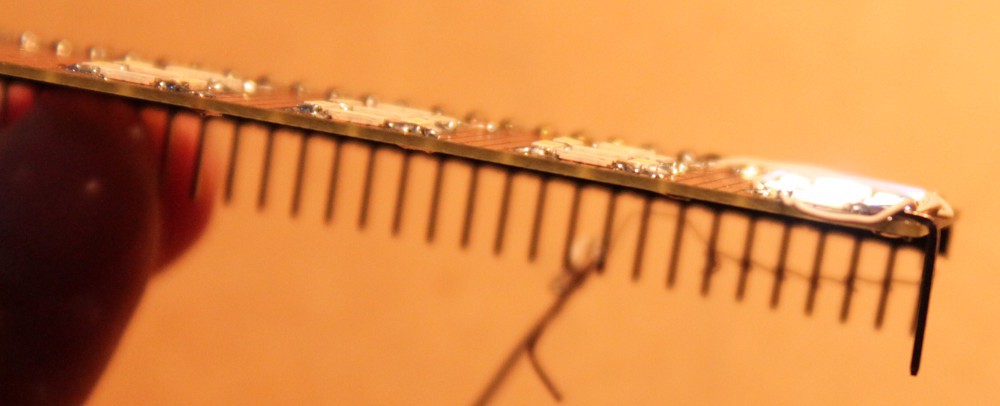
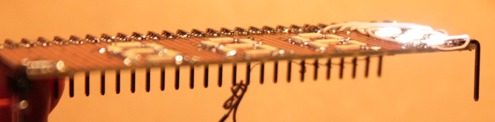
Before I wrote Another way to decode 7 segments displays, I had already soldered a little pre-prototype to test the voltages and visual results. Soldering the 28 LEDs was a bit delicate so I postponed the wiring... until now, I finally brought one digit to life (the others might come, who knows ?)
This results in a little module, sawed off from some SMT proto board that is quite thin (0.8mm incl. copper). The LEDs are thin too so the module is ... thin (about 1.5mm without the tiny wires). It almost looks and feels like an LCD glass :-)
![]()
![]()
So this part of my requirements is reached, the hex display will be modern and thin ;-)
The LEDs are in series with 100 Ohms to balance the luminosity. This might not be necessary but, as we'll see, maybe not...
The LEDs start to shine at 2.5V and are pretty luminous at 2.7V. A single 7-segments digit draws about 50mA at 3.3V and it's VERY bright, almost blinding.
![]()
If I implement the system described in the previous log, I'll have to "undervolt" the Flash. The AM29LV160DB is rated at 2.7-3.6V, so now I have to find a 2.7V regulator...
The LEDs are not rated for 2.7V, so they might vary in luminosity. The 100 Ohms resistors (0603) are kept to balance the brightness. Maybe a higher resistance (around 5K ?) will work better and allow 3.3V operation ?
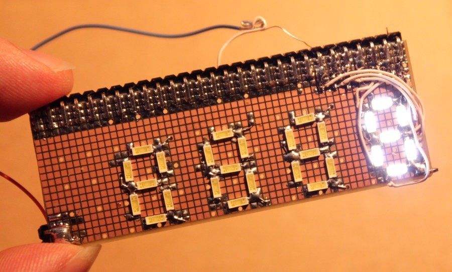
I didn't plan the pinout correctly so the digits are not centered on the board. I'll have to make a new one that shares one pin with two segments, so I can prototype the proposed multiplexed system. Digital dimming will also be useful, I see :-)
Placing a sheet of paper is a bit easier for the eye but I have to experiment more. It's far from perfect but very encouraging :-)
Update:
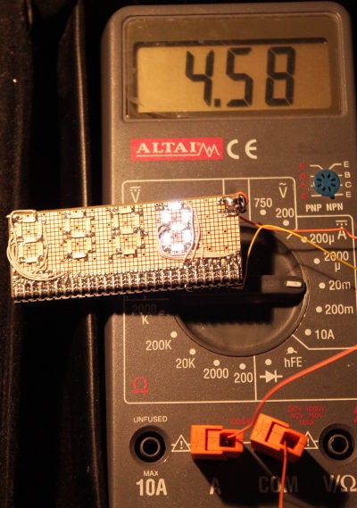
I wired another digit with 1K resistors and the results look good, pretty luminous but not too much and there is some headroom for digital dimming.
A whole digit uses 4.5mA (full on), a couple will draw 9mA max, this is reasonable and will decrease with duty cycle and displayed values. The Flash's output drivers will drop the voltage a little, too, so I rounded 4.58 down to 4.5.
![]()
This is significantly better than the TIL311 :-)
-
Counters, counters, counters...
12/01/2015 at 18:44 • 0 commentsI know it's getting out of hand...
![]()
In the beginning I decided to implement the YASEP's registers as counters, which saves some cycle time. This significantly boosts the system's MIPS/MHz ratio so I got a bunch of 74HC193 counters.
And why not use them for other purposes in other places ?
This time the victim is the FIFO of P1A: the nibble-wide shift register is cool but what if you want to input consecutive data ? How often do we use consecutive addresses ?
A preloadable counter is required. Actually, it should be able to choose its input from the previous hex digit or one of the available bus values (coming from P1B ?) so you can quickly input a bus address, type data in, and move to the next address...
Why not implement a separate "address" register/counter ? That's interesting but I also want to increment/decrement a value that is already present in the FIFO.
But the 74HC193 is not very cooperative. It's actually good at counting but the preload and the timing are a mess. The '193 works as a "transparent latch", not a D-latch which makes preloading awkward, but shifting even more !
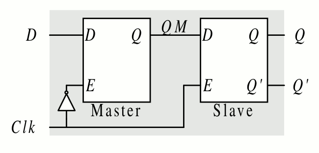
I wouldn't write this log without a clever solution. And this times it comes from the 74HC573. I favor the use of the 574 because it is a D-latch but this time, the 573 transparent latch comes to the rescue. In this case it's even a perfect fit because the /PL input (preload) of the '193 has an opposite active polarity to the 573.
This is pretty cool because together, they make a D-latch:
![]()
(see www.cs.ucr.edu/~ehwang/courses/cs120b/flipflops.pdf )
The "master" is the '193 which can be updated at will, the /PL input remains high and keeps the output stable, while the LE input (latch enable) stays high too, putting the '573 in transparent mode. The counting effects are immediately visible to the outside. There is no need of an inverter, unlike the above diagram :-)
The '573 also helps with multiplexing, thanks to the /OE function. The counters can be loaded with any data coming from another tristate bus.
Apparently I'll have to totally redesign the P1A board and unsolder the already existing prototype...
-
Another way to decode 7 segments displays
11/29/2015 at 20:19 • 6 commentsUpdate: this is now a subproject, moved to #DYPLED
They say when you have a hammer, everything looks like a nail !
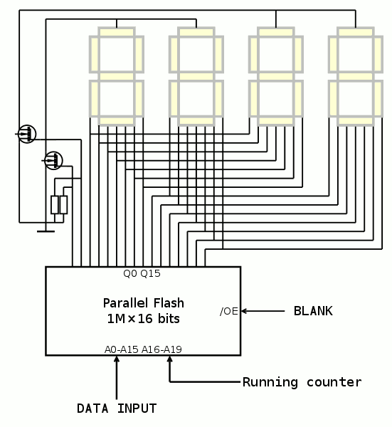
The multiply unit has been replaced with a 1M×16 parallel Flash device. Only 17 address bits are used but when you find cheap trays of these parts, you don't care.
Since I successfully programmed some of those chips, I see other places where it could be used and one of them is none other than the infamous 7-segments LED decoder...
Overkill is fun but the question of price remains. The system with Shottky diodes+74HC154+74HC273+pull-up resistors costs about 0.5$ (in bulk). This can drive one digit, and can be multiplexed for maximum reuse.
Multiplexing can be done with a couple of 74HC153 (dual MUX4) to select one nibble in a 16-bits word, so it adds about 0.3$. Furthermore there is only one 7-bits output and this increases the multiplexing speed.
Now let's suppose a 1M×16 Flash chip costs $1, that's marginally more expensive than the previous circuit. There are 16 outputs which can drive 2 digits. 16 inputs can read a whole bus at once, no need of an input multiplexer. Another address bit can be used to switch between the high bit and low bit so a couple of (cheap) MOSFETs is enough to drive a full 28-segments display (an oscillator is required though, 4 phases is better to reduce phantom lights).
Some more dirty thoughts come while drawing the schematics. For example there are 2 unused outputs. These could be used to drive individual MOSFET gates and save an inverter. The /OE (output enable) would act as a "blank" input and there is only a need for an external oscillator (1-20KHz).
The unused inputs now can serve for sequencing the transistors and even add some luminosity control. The 4 remaining address bits are tied to a 4-bits running counter : the slowest signal goes to A19 which selects the high/low part of the display, the others control the blanking time. Only the code 000b will output data so the LED's duty cycle can be 2×, 4× or 8× according to which of the inputs are grounded.
These features depend on the availability of the running binary counter but it comes "for free" on the P1A/B boards (a wide range of frequencies is provided).
Smart coding will also help: the leading zeros can be removed without extra wiring/electronics.
![]()
Dimming will also come from the control of the power supply's voltage, the parallel Flash should work between 2.7 and 3.3V but going too low will show individual LED mismatches. I don't even use current limiting resistors, this saves soldering time (and there is digital dimming). I didn't show the decoupling caps.
Routing will determine which Flash pin goes where. The above diagram shows that each half is assigned to the Data output but this is not necessary. Routing can be easier if a Dout pin goes to adjacent segments.
What other feature can be extracted from this circuit without adding a part ?
Update: The BLANK signal should go to /CE, not /OE, and the MOSFET's pull-down resistors are not needed since the LEDs will not be driven anyway.
-
A reasonable discrete ALU ?
11/29/2015 at 18:51 • 0 commentsIn a precedent log (What chip(s) for the ALU ?) there was the question of implementing the ADD instruction (all other ASU opcodes are derived from this). I have found some MSI and LSI chips for this, I even considered using Flash or SRAM for this purpose (128K*8 for 8+8+carry) but it doesn't fit with the spirit of the project.
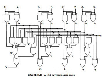
I finally found satisfying explanations at http://integrated-circuit-course.blogspot.fr/2015/09/adderscarry-look-ahead-adder.html
I like that it is well organised and I can almost "see" the DIP chips: one 74HC08 and one 74HC86 for the top row, one 74HC86 for the bottom row, generously spray more HC08 and HC32 for the OR, with other references for the higher input counts (74HC21 dual AND4 and the like, find more at https://en.wikipedia.org/wiki/List_of_7400_series_integrated_circuits)![]()
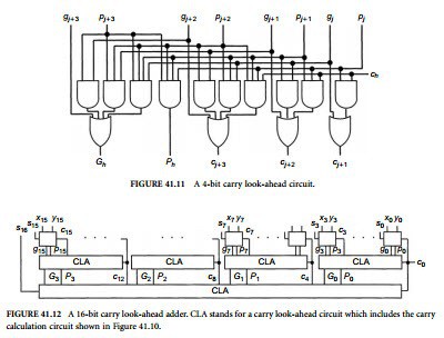
The proposed construct is interesting, the fanout is reasonable and the bottom picture shows that a 16-bits adder is made of 4+1 Carry Lookahead logic blocks.
I don't see where this circuit originates from (I find no reference in the blog) but I see it is very similar to others I see in datasheets, but that are less clear (probably too optimised). For example the right-most AND2 of the above picture is duplicated/redundant.![]()
I don't think I will use this for this project version but I will certainly play with it in a related project that explains every gate and signal of the circuits that the Discrete YASEP uses.
-
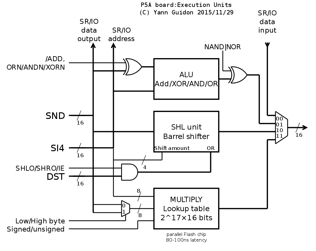
P5A: the ALU/Execution Units (2)
11/29/2015 at 17:53 • 0 commentsThis continues the previous log P5A: the ALU/Execution Units board and the operands
Once the 2 operands are selected and latched, the Execution Units can work. This YASEP has 3 EUs:
- ASU does all the ADD/SUB and ROP2 instruction groups: ADD, SUB, CMPU/S, UMIN, UMAX, SMIN, SMAX, as well as AND, ANDN, NAND, OR, ORN, NOR, XOR, XORN
- The SHL unit performs bit shuffling (see previous logs) such as SHL, SHR, ROL, ROR with optionnal OR for bitfield insertion/extraction. It is also suitable for some Insert/Extract instructions (MOV, IB, EZB). ESB (Extract Signed Byte) requires a little bit more logic.
- The MUL unit is simply a multiply table in this implementation, stored in a 128K×16bits Flash memory. Signed and unsigned results are stored. A MUX2 at the input saves some instructions when computing larger numbers.
![]()
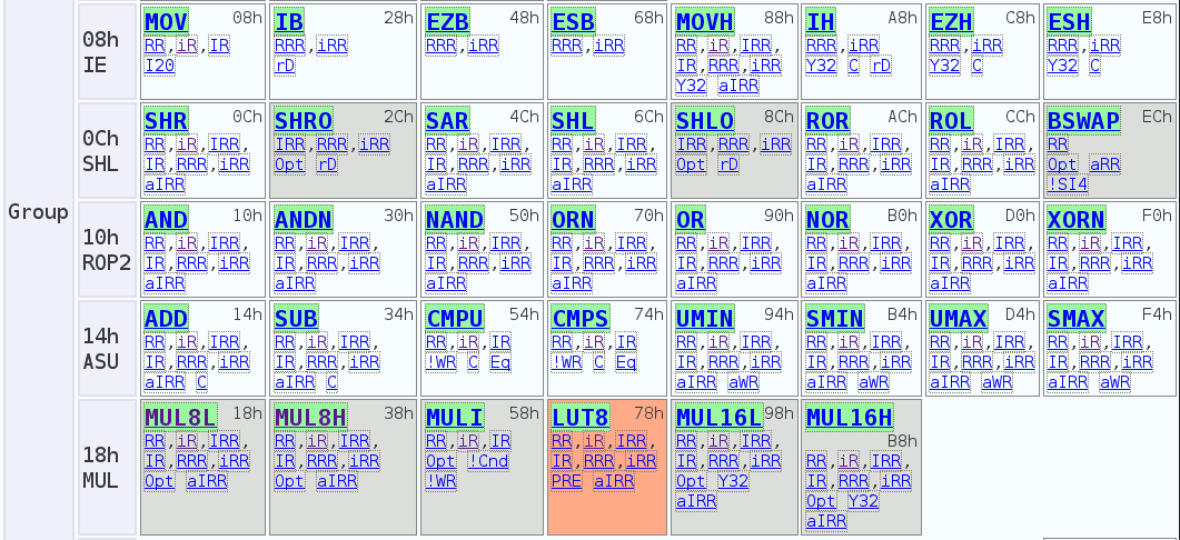
Overall, these 3 units perform most of the defined opcodes:
![]()
The P5A board has another distinctive feature: this is where you plug all the extensions, including SR (Special Registers) or IO (external memory, peripherals...). A MUX4 steers all those data to the output (8× 74HC253 with tristate output)
-
What chip(s) for the ALU ?
11/29/2015 at 05:04 • 0 commentsThe Arithmetic and Logic Unit (ALU) adds, subtracts and performs boolean operations on the operands, so it's more or less the heart of any computer.
This project has two versions: the prototype stage that mixes 3.3V and 5V chips, then the final circuit with 3.3V chips only (for lower power).
Finding ALU chips was a weird experience but it was not too hard. I did not consider implementing a full adder with individual logic gates, it would be really too hard, slow, error-prone, confusing...
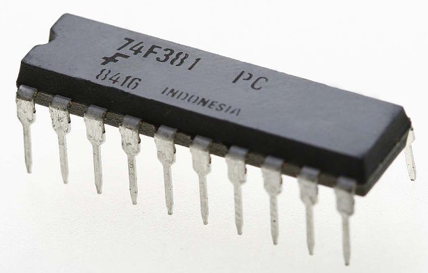
I found several 74F381 online, for about 1.5$ each.
![]()
These are fast 4-bits adders with AND/OR/XOR. However, despite a carry input, there is no carry output for cascading.
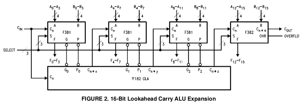
/Generate and /Propagate are available but they require other support chips. The Datasheet from Fairchild mentions the 74F382 but I have no idea if/how I can find one...
![]()
Being a F-type chip, the power consumption is not negligible : about 60mA each (like one TIL311 and 4 are needed). The F-type signals work with current, while the HC work with voltage, so pull-up resistors are needed (more power draw).
It's also a pretty rare part, now, with no SMD version in sight.
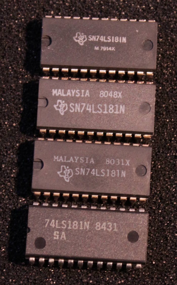
By chance, I found a few 74LS181 in an old local store.
![]()
Can you believe that they have been manufactured more than 30 years ago ? How long have they been waiting in a box/tray/shelf ?
The '181 has a carry output (inverted) so it's easily cascadable. The function set is quite flexible so it's often used for DIY projects. But it's not an option for the final version...
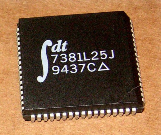
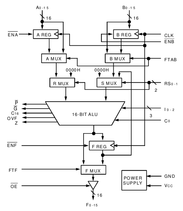
SMD versions of the '181 are too rare and too expensive. DIP versions are in the "a few dollars" range so a 16-bits ALU costs more than 10$. Luckily, I have found another more advanced circuit: the IDT7381 16-bits ALU.
![]()
It's a PLCC chip so it is "mostly" SMD (on the "thick" side of "thin") but the cost of a 16-bits slice is about the same as a 4-bits only '181. The operations are identical to the 74F381 but in CMOS and the Carry Lookahead is integrated (there are outputs but one chip is enough). It's pretty fast, the sum/difference is output in less than 30ns. Power consumption is lower, too, worst case 60mA for 16 bits.
![]()
But this part is also obsolete, available in limited quantity, and it's a 5V part. There are one or two equivalent products but I wouldn't bet on their long-term availability. At $3/pc, it's great for hacking stuff but there must be a better way.
It doesn't look possible to reach $1 for a 16-bits ALU (with added constraints of decent speed, ultra low profile and 3.3V supply). However around $2, there are more possibilities using CPLD/EPLD. The data use 16×3 bits, 48 input/output pins, plus all the control and status signals, at least 68 pins are required and the cost is still high.
But I have found low density FPGAs: the A3P030 is the smalled of the family with an easy to solder TQFP100. It's more or less equivalent to a 256 macrocells CPLD (768 LUT3), works at 3.3V, and I have all the hardware and software tools. I can even reuse source code from previous YASEP implementations.
It's weird that the project has gone "full circle" and returns to the chips it tried to avoid. However, the ALU is a special kind of circuit that is very hard to do well and cheaply. An exception to the rules can help progress while respecting the other design constraints. The A3P030 doesn't have SRAM blocks, a PLL or some other features from the larger chips so there is no risk of feature creep.
A "discrete" version of the ALU would be implemented in a different project. Because it uses many types of logic gates, it will be hard to find suitable and cheap ICs. Unlike the SHL unit, the structure is not very regular and the design would be very hard. Several years ago, I have fiddled with a 32-bits adder at the gate level and it was not a pleasant experience...
Update (2016-01-06):
I found some 74HC283 :) It's a plain dumb 4-bits adder with Carry In and Carry Out, straight-forward to cascade. Quite slow but convenient and no voltage translation chip is needed, since it works with the same 3.3V levels as the surrounding circuits.
The boolean operations (AND/OR/XOR) require external chips but that's not a real problem.
-
P5A: the ALU/Execution Units board and the operands
11/28/2015 at 21:55 • 0 commentsThis board has not been described before but there is enough progress to do it now.
P5A has several functions but mainly, it's what transforms the operands into a result. This includes computing (add/sub/mul/SHL...), updating a couple of condition codes, assembling the operands from the different fields and even some I/O.
The board's dataflow starts with the SND and SI4 operands, which are correctly selected and latched. SND and SI4 are available on the read buses only briefly, because once they are read, the sequencer will read DST and CND (destination and condition) right away (when applicable).
SND is the operand that can be negated (for boolean operations, as well as SUB and derivatives like CMP, MIN/MAX...) so its value is latched right at the SND data read bus. The SND address (4 bits) may be reused as a destination address for the short instruction forms (but this is handled elsewhere).
SI4 is the operand that may be a register or an immediate value. Immediates may be 4, 6 or 16 bits wide in YASEP16, always sign-extended. Some MUXing is required in front of the latch. The MUX is controlled by a few bits of the instruction.
SI4 is a bit tricky because its value can come from both half-cycles of the instruction: a register value (form RR) or a sign-extended 4-bits immediate (form iR) can be written at the end of the first half-cycle, but this value can be overwritten if a) the instruction is a long immediate (form IR or IRR) or b) an extended form with short immediate (form iRR)If the instruction is short, the SI4 register is not changed. If the instruction is long, only the 12 MSB are changed because the fields are designed to minimize bit shuffling.
The 4LSB are latched from a MUX2:
- when the Imm/Reg flag (instruction bit n°1) is 0, the SI4 read bus (bits 0 to 3) is chosen,
- when Imm/Reg is 1, the SI4 field (address field from the instruction, bits 12 to 15) are chosen.
The 12MSB use a MUX4:
- When the Short/Long flag (instruction bit n°0) is 0 (short form), select either the SI4 read bus (bits 4 to 15) when Imm/Reg is 0, else copy the SI4 adress MSB (sign extension).
- When S/L is 1 (long form), copy the instruction's bits 16 to 27 when Imm/reg is 0, else copy instruction bits 16 to 17, then pad the MSB with bit n°17 (sign extension)
I apparently forgot the RRR form but that's just a it more decoding logic, no datapath modification. Sequencing will be a bit tricky too but not impossible.
One extra MUX2 layer could be added to overcome the main issue of the YASEP ISA. Relative jumps are limited by the small width of the SI4 operand in extended form. The new ISA (defined in 2014) extends the imm4 field from 4 to 6 bits with a clever reduced-size "update" field but the range is still +31/-32 bytes, or +7/-8 long instructions only.
The range can be extended in two ways but they both need extra logic in the critical datapath to detect a iRR add with PC as destination and source (ADD x PC PC condition)
- The range can be extended from +7 to +8 by adding +1 through the carry input when the imm6 field is positive (bit n°5='0'). This makes sense because "ADD 0 PC PC" is useless.
- The range can be doubled with a MUX2 on SI4, that shifts the imm6 operand by one bit, because instructions have an even number of bytes.
These two methods are complementary but have side effects when put together. To effectively increment the shifted Imm6 value, the LSB (bit n°0) must be set to 1 so the carry-in of the ALU will ripple to bit n°1.
However, detecting the right condition uses gates and takes time. The first conditions are evaluated while the register set is being read so it's painless:
- Opcode : Add
- LSB=11 (extended instruction)
- SND address=PC (0)
However the second half of the instruction becomes critical:
- Aux flag (bit n°20) = 1 (imm6 present)
- DST = PC (0)
- MSB of imm6=0 (for the carry in and LSB setting)
Since this condition can only be found after the first nibble of SI4 has been latched, the shift must occur after the latch...
Discrete YASEP
a 16-bits YASEP computer (mostly) made of DIP/SOIC chips like in the 70s and 80s... with 2010's twists!