 Eric Hertz
I've only *just* begun looking into the TMS9900 architecture; a 16-bit processor used in the TI/99-4[A] home computer during what otherwise was the 8-bit era.
This thing had a steep hill to climb... imagine a 16-bit computer with only 16 bits of address-space. Heck, even most 8-bitters could address 64KB! And adding paging to those was not at all uncommon, nor particularly difficult, wherein 4MB or more was definitely doable (see e.g. #Vintage Z80 palmtop compy hackery (TI-86) ) on even 8-bit systems.
So, of course, most of the vids I've seen on the matter basically blame its 16-bit address-space for its not having been used in basically anything other than the TI99, even though it was in the running for the IBM PC, before they decided on the x86 architecture (with 20 bits, 1MB, 16 times the address-space!).
So, I was pretty quick to dismiss it, myself, especially since I don't have one in my collection.
But, something really unusual caught my eye...
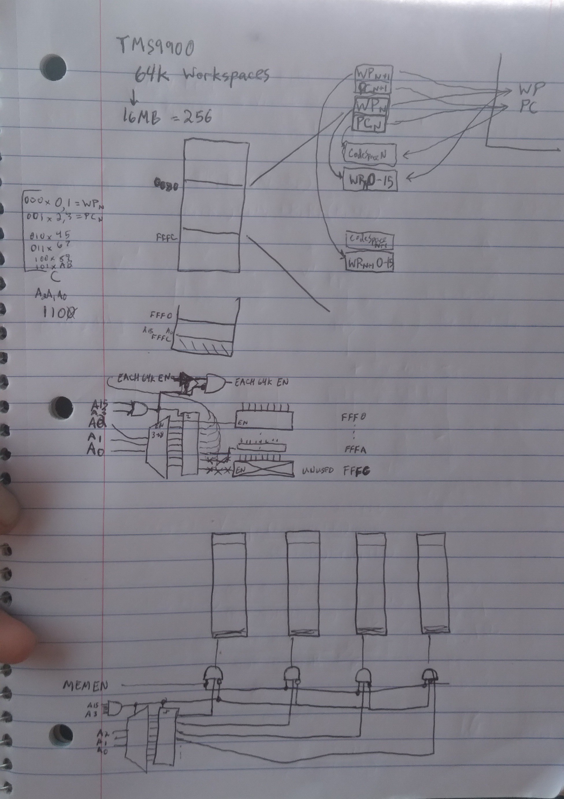
Instead of having its registers internal, like most processors I've seen, it has its registers located in the external RAM.
Even weirder, it has Multiple Sets of those registers, instead of using a stack. This allows for really fast context-switching. Calling a function, Handling an interrupt, surely more... No Pushes/Pops required. The "branch" (aka "call") instruction merely copies three bytes from RAM to its internal registers.
Now, I can imagine that can be pretty limiting in cases of recursion. (and what keeps track of where to return to? I haven't read closely enough to know, yet).
But...
This got me thinking...
In order to switch contexts, it loads the Working-Register-Pointer, from a lookup table, from RAM.
Now, if, say, you were to watch the memory-bus for accesses to that lookup-table, you could automatically switch to a different 64K page of RAM.
I've come up with a simple circuit to do-so.
To keep it really simple:
If you assume that any page-switch is essentially a completely separate "program", then the page's entry-point working-registers could all be located at the same address, (ala the reset address), and there needn't even be actual memory/registers to store each page's working-register-entry-pointer.
This is WAY simpler to implement than page-swapping on most CPUs I've seen (and, really they're not so complicated).
So, basically, all it takes is dedicating, say, addresses to this "page-swapping," an address-demultiplexer, an 8-bit register/latch, and a few AND gates.
Now you've got multitasking up to 8 separate tasks, each with 64K to work with.
Adding RAM/Registers for each, for the sake of saving/restoring and/or calling a specific function within another page shouldn't really need much additional work, when you consider that RAM /will/ be at that address, as well...
(I explicitely disable them in my schematic, during accesses to the page-lookup-table, But, maybe the First page should always be enabled during those accesses? Simply remove the disable-input to its 3-input AND).
...
So... Why?
Well, obviously multitasking... And comparatively huge amounts of RAM.
But also consider hardware is memory-mapped I/O... Each piece of hardware, /and its drivers/, could be in a page of its own (or a page dedicated to all the drivers/hardware). You've got to call its driver-functions, anyhow, this would be just as fast, either way, and free up RAM/address-space for the programs themselves.
Here's another thought: Address-decoding requires a lot of circuitry... But, here, each "page" is selected separately; it's already mostly decoded. Maybe 16MB on a 3MHz CPU is a bit silly, but 256 pre-decoded addresses would sure make adding custom hardware easier. Each add-on-card could be in its own page, address-decoding circuitry becomes easy-peasy.
I dunno. I guess with all the hacks used in systems of the era, I'm kinda surprised something this easy to remedy was overlooked, and its "killer."
Discussions
Become a Hackaday.io Member
Create an account to leave a comment. Already have an account? Log In.
I hate kit, i need full working device and way to replace firmware.
less ram? slowly cpu ? no problem, every can use assembler or write a backend for llvm ;-)
problem is with working device, power, network etc.
i need editor, sharing data trought my desktop workstation and computer that working 10 time longer than my laptop
Are you sure? yes | no
All this,and more, can be achieved with a 16-bit processor!
Are you sure? yes | no
I wrote, no problem 8 or 16 processor or 64
no necessary '!'
necessary a week working time on one chcarge
Are you sure? yes | no
I hate to say it, my friend... But I cannot parse any of what you're saying...
Are you sure? yes | no
ok
forget. (i need only computer with working time more than my laptop , power is a key) my english is bad
Are you sure? yes | no
Back in the 1980's I used to work on equipment in a semiconductor fab facility. The diffusion furnaces used the TI TMS9900 processors. The furnaces were made by Thermco. Four tubes to a rack and a separate processor per tube. I "think" the user interface was via a serial terminal (custom). The 9900 boards lived in a 19" chassis. There were a number of custom interface boards to read the thermocouples, drive the gas valves and the power switching for the elements.
I remember studying the 9900 processor at the time and thinking it was an exceedingly odd piece of work. Instead of having memory mapped I/O, they had some kind of serial shift register thing. Kind of SPI ish.
That was the only place I ever saw the 9900 processor used in the wild.
Are you sure? yes | no
Interesting! So they did manage to get in *somewhere* besides the TI-99. And, it makes some sense it'd be in an industrial control setting, if I understand the motivation behind its being essentially a single-chip version of the architecture they'd already been selling to such markets.
I saw that weird shift-register thing, and frankly didn't even begin to grasp it. So, that was intended for I/O, then... I guess that kinda makes sense... I suppose shift-registers were about the same cost as an 8-bit latch, and no address-decoding necessary... But, wow, it must've been slow if you needed a lot of I/O's! I'm guessing, in the industrial control world they probably intended it mostly for relays, lights, and switches, as opposed to, say, reading a bunch of 12bit ADCs. Though, I suppose it might've also interfaced with terminals pretty easily. Good call comparing it to SPI. Maybe it was ahead of its time...?
Are you sure? yes | no
Oh! Fascinating excursion! I didn't work with the TMS9900, but I do remember it was essentially a single-chip version of the existing TI-990 minicomputer (which was successful in the market of data-processing-for-the-petroleum-industry, which apparently was TI's bread-and-butter). Purportedly, TI had a corproate philosophy of having one single computer architecture to rule them all. So that's where the distinctive features (like the memory as registers, working sets, 16-bit address space, etc) came directly from.
The memory-as-registers approach was not unique with this part. Aside from other minicomputers, the zero-page addressing mode of the 6502 is essentially an in-memory register file since you can do all the math ops and whatnot. No working set there, though. Also the 8096 register file was intrinsically mapped to memory (but that device was a microcontroller with on-chip RAM, so not maybe not as interesting of a parallel). As you guess, as things progressed eventually CPUs would outpace memory speeds making this not viable.
Poor old TMS9900. The 16-bit address bus was pretty short-sighted, but hey 'one architecture to rule them all', right? And of course, it came in a 68-pin DIP! So more lines will probably need some sort of multiplexing for the packaging options in those days. The lack of peripheral chips was not great, either. After losing the IBM bid, they did the TI/99-4 which was kind of a disaster as a design. There was 256 bytes that was directly accessible to the processor (for things like these register sets), but regular DRAM access had to go through the video controller for some reason and was slow. Wut? (to wit, the TI-99/4 was a merger between a group that was already working on a game console and some guys in the business division, so maybe that's why the dram access went through the video controller).
But a nifty bit of history!
Are you sure? yes | no
Hey Ziggurat29, was wondering what you've been up to. Thankya for the history!
Indeed, I heard that the limited 256 bytes of RAM was due to the speeds required for the working-registers... Larger RAMs that fast were just not affordable at the time.
So, in a way (not understanding the specific Video chipset at all), it makes a lot of sense that a "graphics card" with its large array of RAM for a framebuffer or character buffer (40chars x 25 would require 1KB of RAM, Many Times the CPU's RAM!)... Lemme start over. Since the graphics "card" has to have all that RAM, and make it accessible to the CPU, it makes some amount of sense to use that already-existent large-memory-interface system as a general-purpose memory-controller, as well. Weird concept: Use the GPU card's memory as system memory.
OTOH, I'm pretty sure I saw the TMS9900 has wait-states, too, so slower memories *could* have been directly attached? Hmm.
Interesting about other CPU architectures with external registers. Am not surprised it didn't last long. Even if RAMs were fast-access enough to keep up, I'm betting it takes far more clock-cycles for a single external read/write than it would internally, due to the order of setting up the address, setting the Read/Write pins, clocking in the data on the appropriate edge, and so forth. No address to load for an internal register, and the order/timing of those things could just-as-well be handled internally not delayed artificially by clock edges, but happen as quickly as possible with gates' propagation-delays.
Still, as far as new-retro goes, I see the TMS9900 as an interesting path. What could've been, had things been slightly different. (I kinda want to throw today's fast/large SRAMs at it!)
The thing I really find intriguing about this working-space thing is how it pretty much inherently lends itself to paging. The same act of switching workspaces, which was designed for its speed, /also/ enables page-switching, with zero added overhead. Surely someone's thought of/implemented it! Really, I'd think it even more cycle-efficient than x86's use of segment-registers, since calling a function in a different segment would require an additional register-load. Here, just call that function like any other (as long as its workspace-pointer is in the address-space dedicated to page-swapping... I used addresses FFF0-FFFC in my circuit, for easy decoding).
Yeah, 64-Pin DIP, hah! Believe it or not, it has a couple No-Connects!
Good to hear from yah! I've got an unknown surplus gizmo coming in the mail soon, with RS-232 and GPIB that speaks to me of the 8, possibly 16, bit vintage... The wealth of knowledge you've shared of such architectures, disassembly, etc. at #OMNI 4 - a Kaypro 2x Logic Analyzer and #Vintage Z80 palmtop compy hackery (TI-86) made this hard to pass-up. I'll let you know what I find!
Are you sure? yes | no
If you've got an actual chip on-hand, why /not/ play with it? It does have a wacky clock scheme, so hope you have a generator chip, too. And the multiple supply rails -- blick.
I certainly do not know for a fact, but I suspect the 'access main memory through the graphics chip' might have been an artifact of the TI99/4 resulting from the merging of the game console group with the business computing group -- possibly aspects of the design already existed in the console group by the time the computing group was merged in. But who knows? Incidentally, despite the (rather dramatic) failure of the '99, part of its spirit lived on through its video chip -- that was the basis of the video portion of the MSX standard. MSX was not big here but it was big in Japan. Basically, a Z80 strapped onto the TI video; lol.
Your hardware-assisted bank switching scheme is indeed interesting. If I read you correctly, some hardware on the side watches an address to infer that the register file is changing and then sets up a concomitant bank switch to match. Very neat and tidy!
Alas, poor segments -- I remember them, Horatio. They certainly weren't invented with Intel chips. Like the registers-in-ram concept, they were a systems design concept from the mainframe mindset. Two major competing ideas were segmentation and virtual addressing. We know that virtual addressing won in the end, but this wasn't clear in the 70s-80s. Poor Zilog couldn't decide and produced two versions of its 16-bit offering -- one segmented and one non-segmented. Those failed due to bugs and performance so how the mighty did fall but Zilog lived on in producing peripheral chips. Similarly, TI gave up on general-purpose CPUs and rose from its own ashes with the wildly successful TMS320 series which was a whole market category of their own creation.
Speaking of segments, there was a much greater cost in loading them than what might seem in loading a value into a register. (well, on the 286 and above). Loading a segment register then incurred a lookup into a descriptor table which then had to be validated as safe to load for your current ring of protection and this incurred many more hidden memory accesses and was /expensive/. In the real world, I had written a FIR filter routine in C that was non-performant. Looking at the generated assembler, I could see that it was loading a segment register (ES?) when bopping between coefficients and signal data buffers. I managed to hack that gently to coax the compiler to not do the segment loads and sped the thing up by a factor of 70x! So what took a minute now took a second. (The 486 largely obviated that cost through descriptor caching, but this was 16 MHz 386 days.) Don't even get me started with 'call gates'.
If you /don't/ have an actual TMS9900 on hand to play with and are just curious to study ancient microprocessors, you might give the Intel 432 a look. It was originally called the 8800 (in the obvious naming progression) and was started in 1976 and was fully 32-bits from the beginning. When Intel realized it was going to take a bit longer to develop and saw competitors in the meantime delivering stuff to the market, as a knee-jerk reaction they made the 8086 as a quicky just to keep in the game. The rest is history on the 8086 line, but it's interesting to note that it was never intended to be what it turned into. Meanwhile, the 432 was something /really/ far out. But ultimately it failed (and quickly), though it was pretty audacious that something of that scope was even attempted in 1976. Worth a look.
Well, fun times. I still intend to attempt surgery on the calculator to resurrect it, but I've got work stuff ahead of that for the near term, alas. I'm super interested in hearing all about what new vintage junque you are about to acquire!
Are you sure? yes | no
Briefly (hah!) before an errand...
Ah Hah! I spotted a fatal design flaw in my circuit, but the fix is not difficult. Definitely do not commit the bank-switch when the address is unstable! Latch that register off another signal (ala /RD)
I don't have a bare TMS9900, though I do have a TI-99 a buddy gave me along with a bunch of other stuff long long ago, but long after I'd developed my affinity/nostalgia for other systems, so I'd planned to send it to a thrift-store. At the time, if I'd had this idea, I might've stripped its CPU and tried a homebrew. Heh, probably a good thing I didn't understand CPUs to that level back then! Still, I might be tempted to see if it's in a socket, next time I unearth that machine.
I tried a Youtube search for homebrew TMS9900 machines, they are few and far between compared to z80 homebrews. But one odd-to-me result (which you just explained) was that the suggested searches didn't even include TMS9900, but /did/ immediately bring up several suggested searches for other TMS99xx chips. I clicked-through thinking maybe the part number was a later 9900 model, only to find something I thought very strange... A bunch of homebrew Z80 machines using the TI-99's graphics chip. Wha?!
Ahhh, now I get it. Thanks for explaining!
BTW, if you haven't already stumbled on the Z80 homebrew youtube rabbithole, you might want to avoid it... There's probably more interesting footage in those realms than hours in a lifetime.
Are you sure? yes | no
lol; yes I avoid YouTube whenever possible. Most videos are ploddingly slow, and with text I can control the pace. Plus text is random access and video is sequential access (and rarely indexed).
You might have some fun homebrewing a 68000 machine, but that cpu design was so sane that you might find it a bit boring.
You are getting very adept at the low-level hardware stuff. You might consider at some point picking up Verilog and using an FPGA. It's been on my bucket list for some time now, and the cost of entry is so low. E.g the EP2C5
http://land-boards.com/blwiki/index.php?title=Cyclone_II_EP2C5_Mini_Dev_Board
but time is, alas, the elusive commodity.
Are you sure? yes | no
LOL at sane processors. I did, actually, invest in a Palm V PDA with every intention (being *so* cheap these days) of stripping its backlight for the TI-86...
But, having it in my hand brought back fond memories, and now I just don't have the heart to gut it. Besides (thankfully, maybe) its screen is slightly too small. But that means... I've a 68000-based vintage palmtop to maybe hackify.
I can't quite wrap my head around it, though... I really liked Palm OS. Did you know it had ResEdit just like Pre-OSX Macintoshes? Seriously, It boggles my mind they did away with resources, seems like such a backwards step. (Speaking of sanity)
Otherwise, I've a 68040 in my family's very first compy, but there's no way I'm hacking that... (is there?).
I dunno, something about the insanity of these other processors is what draws me to them. How do you get a system limited to 64K to use Megabytes? How do you make use of weird quirks like a system limited to 256-IO ports which just happens to spit out 65536 addresses during IO? Or Refresh, how handy could that be for *other* things?
FPGAs... Everyone suggests I should get into FPGAs... I just don't see the draw, except in some end-product, maybe. And even in most of those, I think they're over-used. The lack of standardization is a huge turn-off. Do all that hard work for an Altera part, then good luck porting it to Xilinx. Or even to a new Altera part in five years... In my experience, regardless of the brand, you'd be lucky if the new toolchain will even support the old files, nevermind the old chip if you need to do a bugfix... and even luckier if you can still get a copy of the old toolchain, nevermind be able to run it on a newer OS. And now with specialized outputs? Hah! Good luck running DDR2 on a new device. Nah, they mightaswell be locking yah in like Mask ROMs.
Not At All impressed.
Oh sure, how else you gonna run LVDS at 100's of MB/sec? Right, they locked us in. Heck, if they had the guts to sell "Mask-Programmed FPGAs" as though nothing more than e.g. simple cross-brand pin-compatible serdes chips, I might think about buying them for purposes like those... But I really am not fond of how everything seems to be going the way of the brand-specific epoxy-blob. What happened to the era of second-sources? Just synthesize it!
It's, what, nearly 40 years since the Z80 was a gamechanger... And yet it's still in use in products made today, it's been made by countless manufacturers, in countless new and faster forms, you can even buy the original part new. Same goes for TTL, and *most* of the processors of that era. And did I mention the wide selection of toolchains, and device-programmers? Let's see if *any* FPGA can claim the same for merely 5 years, then maybe I'll start thinking about 'em. I've yet to find it even with simple PALs.
...
I somewhat agree about the video thing... Random-Access of text is not how I'd thought of it before, but yeah, that's very true. Though, vids have other aspects... "A picture's worth a thousand words" then a video... well, it conveys a thousand pictures; albeit the million extra words may seem rather irrelevant to the topic at-hand... Maybe conveying more about the person than the thing they're discussing. I think there's value in that; but yeah, it can make the gathering of project-relevant info quite a bit more difficult... No "search"!
I am impressed, though, by the wide range of folk doing stuff like this. Many coming into it as though new to electronics, others who are clearly experts, some teachers, some artists, some just want their efforts to hang on a fridge (be seen). I wouldn't mind being able to give them all more of my time, but I've got ideas need doing, too! Heh! And, dagnabbit, every time I watch one of those vids, I get a slew of new ideas need doing, as well.
Are you sure? yes | no
I have a Sony Clie from circa 2000 which I got fully for the intention of developing apps, but I got quickly frustrated with PalmOS, so I didn't pursue it further. But there was an appeal to those devices. Now I guess the functional analog is the modern smartphone.
You mention of the 64k I/O ports when documented as 256 I think I just figured out a couple weeks ago. Coincidentally, I just built an 8080-based system, which of course the Z80 was to be binary compatible. This forced me to read the 8080 docs, and those specify the 8-bit address space. But in reality, the 8080 puts a copy of the 8-bit address also on the upper 8-bits. Not really useful. So I suspect Zilog figured why not put B there? And then be (BC). I think they chose to document that it's an 8-bit IO space to emphasize compatibility with the 8080. But it was always a mystery to me that the Zilog docs also explicitly say 'oh, by the way, the B register is on the upper 8-bits; lol'. So it's not like it was undocumented. It was the worst-kept secret feature.
Man, this 8080 gets hot! I'm a little surprised it works because I bought it as a kid in 1978, and it's been bopping about in a junk box for the past 44 years with no static protection. Hmm! The wacky clock and the 3 power supplies and the various separate support chips makes it pretty clear why the Z80 ate their market. The 8085 was clearly intended to be Intel's answer to the Z80, but I think the battle was lost by the time it came out. And then Zilog botched the 16-bit scene, so how the mighty fall.
FPGA interests me from the notion of creating custom CPUs. But I guess that hasn't interested me enough to do that yet. I have those boards I referenced for a couple of years now and they remain on the shelf, waiting for their time at-bat. Perhaps in a shorter time than my 8080 from the '78.
Video is useful for showing technique, like how to make an omelet. Otherwise, I am a captive audience taking information at the rate the presenter chose.
In other news, I am returning to the land of the employed, and this will alas put a damper on my side projects -- at least until I get my sea legs. Then maybe I'll fix my damaged ti-86!
Are you sure? yes | no
Hah, the comment-thread, as usual, has gotten unwieldy to the point of not being able to refer back to your post while writing this... So, from memory...
LOL at your imagined quote from the z80 i/o docs. And interesting point about the *why*. Yeah, I recall its sounding like it was one of those unintended "features" that just happened to come along with taking the easiest approach. E.G. The hardware already put BC on the address bus for other instructions, so it'd've taken *more* effort to disable B. Then someone was like "well, they figured out how to make use of our dirty secret, let's make it look like we intended it." But, I think I like your version better; a little jab at Intel for doing something completely useless, and finding a really easy way to make it useful, while *also* being backwards-compatible!
Cool you're building an 8080 machine. I've been pleasantly surprised at how many junk-drawer poorly-stored chips still function. I just slapped-together a little binary-counter/frequency-divider from an 8035-based PCB that's been rustled-around with dozens of other old TV boards and such through many moves and many a dig-through. (Remove ROM, insert SIP resistors on data pins and GND, Worked immediately! Got a decent 120Hz signal on A10)
I never did any Palm OS devel, that was before my coding experience... But gui coding is something I've never been good at, and I can imagine it'd be even more frustrating back then. I remember my C class had a gui assignment which used a custom library that did common setup for many OS's, but it was huge and basically did little more than allow drawing pixels or detecting a mouse within its window.
You're right about FPGA's and custom CPUs... They would be by far the best way to iterate a design... I guess I'm not much of a custom-CPUer. Though, my stubbornness about FPGAs still bites me in the A**, since I have a really soft spot for various old LCD, EL, etc. displays, and of course, there'd be no easier way to drive them. My first raster-drawn display driver was mostly TTL, back when I was in my teens... Later #sdramThing4.5 "Logic Analyzer" was a *really* weird way to do it, and inbetween was "avr-lvds-lcd." So, I guess for me it's almost as much about the displays themselves as it is about figuring out *weird* ways to make them work. Part of the reason I got excited about old CPUs, running NOPs is the fact it's a 16bit binary counter... perfect for raster-drawing from an SRAM, heh!
(BTW, did you see my score on the z80-based surplus test-equipment? https://hackaday.io/project/8348-random-ridiculosities-and-experiments/log/206221-another-z80-system )
Congrats on employment!
Are you sure? yes | no
This 8080 build is from a kit, so don't be too impressed, it just struck me as interesting since I never worked on the 8080 before. It's not supported by SDCC, and I looked at making a backend for such, but the project documentation is non-existent for doing so and understanding the source is quite a chore. So this may just be a toy to enjoy as-is.
Ah, the 8035. I myself used the 8749 a lot -- much to the annoyance of my employer and college profs. I think it's basically the same CPU, just with on-chip eprom and may more ram? Can't recall -- that was the late 80's.
Oh, my, on the new find. Very interesting. I'll post more there...
Are you sure? yes | no
Ah, interesting.... I'd contemplated exploring sdcc numerous times, but oddly can't think of whys right now. I do recall being a bit confused about its being both The GoTo, and also seeming a bit rag-tag at the same time. A bit of a chicken-egg question as to how it could be both. I guess that's opensource, when it comes to things that are a bit niche.
Actually that sort of thing is kinda reassuring... A bit like finding a recently-updated site written in pure html. I'll have to ponder that a bit.
I read somewhere, IIRC, that the 8035 is identical to the 8048, except the latter has onboard ROM... which would defeat my purpose of NOPing for the address counter... EXCEPT, that, in their identicality, they both have a (the same) pin to enable booting from external ROM. Interestingly, I also read that some 8035's might've been intentionally relabelled 8048's. Kinda a clever move on the part of manufacturers who could run a batch of custom masked 8048's for a client, and restock a bunch of 8035's in the same run. Aside from that, and NOP=0x00, I know near ziltch about 'em. Which was kinda the point of that endeavor; see if I could put to use an old random uC on its old scavenged PCB that's been sitting in my bin, without having much of a learning-curve. Concept proven :)
Cool to hear you used to work with the MCS48 series. I imagine I'll be using them more, as I think they were commonly used in keyboard controllers(?).
Are you sure? yes | no
SDCC is very ragtag as projects go. Started in late 90's for the 8051 (which I have /not/ worked with), and other folks extended it. It's definitely still being worked on (6502 is being added now), and the design is solid, just undocumented. It's a steep learning curve. So after a few days I shelved it, especially now that the new job is coming up. I spoke with another guy who tried for the 8085 and he said 'talk to the hand', so I suspect he had similar frustrations and he worked on it for about a year on-and-off.
The attraction of using SDCC is that working in C is so much more productive than assembler. And using a compiler that supports modern C is so much more pleasant than, say, firing up Aztec C on CP/M and building on-device. If I were going to do something like a full OS, I'd really rather write that all in C and save the assembler for bootstrap -- pretty much like in the real world.
Yes, now I google and see the 8035 is in the family, just a different ram/rom combo. The '7' in the numbering means 'eprom'. Yes, you can do something and run from external rom and then it's more like a 8035.
Yes, they were commonly used in keyboard controllers; the TRS-80 Model II used one variant, and the IBM PC's used another. They were also popular in traffic lights. I enjoyed them despite their quirks, like the banked memory.
Are you sure? yes | no
Ahh, yes... I had some USB2 microcontroller that was 8051-based and thought to implement some things like a USB/SCSI converter... Didn't want to install/run windows to use the IDE that came with it. But, it took a bit to realize that meant making my own header files, etc. so it never took off.
I do much prefer the portability of C over assembler, nevermind the ease of making changes that might otherwise require changing around registers, etc!
I had an idea, recently, about trying to find the core set of assembly-instructions, flags, and registers available in most (8bit?) architectures; they all seem rather similar. E.G. a jump to a specific address seems almost universally three bytes: Opcode, address-high, address-low.
If there's a common-enough turing-complete set, then a sort of universal assembly language could exist, using only those, and the only difference between an executable on one architecture vs another would be the actual opcode values. (which, maybe, even, could be reassembled on the fly?) It'd be kinda like reducing CISC machines to RISC, so they can all run the same code.
A bit ridiculous, maybe, but then it could be possibly taken a step further to a C compiler that uses *only* those instructions/registers... So, then, works for numerous systems, and a sort of BIOS that standardises hardware-accesses, etc., through function-calls... I dunno, sounds kinda silly, if not unrealistic, right now... Things like interrupts and reset vectors (and methods) varying so dramatically. Then again, the goal obviously isn't maximizing functionality, but compatibility for the sake of the developers... Who really needs interrupts, DMA, etc.?
Heh!
Are you sure? yes | no
Yes the 8051 was the successor to the 8048 line and is immensely popular even to-date and often embedded in other SoCs. I had occasion to delve into an encrypting hard drive of recent make and Lo! and Behold! it is an 8051 core.
Your thinking on the notional universal assembly language is very good and I'd like to introduce you to the dragon book for starters:
https://en.wikipedia.org/wiki/Principles_of_Compiler_Design
The typical design comprises of:
* a 'front end' that understands your high-level language; e.g. 'C' or 'FORTRAN' or 'Java' or 'brainf*ck' (it's a thing)
* an 'intermediate language' ('IM') that is like your universal assembler you mention. it runs on a conceptual processor that has things like infinite registers, etc. Most of the heavy-duty optimization algorithms happen here as well.
* a 'backend' that takes the IM and translates that into machine-specific object code. 'register allocation' is done to remove the assumption of there being infinite number of registers by analyzing lifetime. Where stuff can't fit in your physical register set, a 'spill' occurs to temporary storage, such as the stack or wherever. Also, 'peephole' optimizations are done, which are mostly pattern matching for silly stuff that can and does come out of this translation process such as
ex de, hl
ex de, hl
and replacing that with nothing, or other similar transformations.
So, your idea is /not/ silly. Your ideal /is/ realistic. It's just that this thought has been thunk and there's a huge body of theory already behind it. It's impressive to me that you have intuited this approach. By the way, for whatever reason it's somewhat of a black art despite being very well documented and if you can pull it off you can get a really big salary. So if this is your jag then do pursue it. I would suggest also looking at 'LLVM', which frameworks most of the common stuff above and then you make a 'backend' for your target machine, or a 'frontend' for your target language. It's also sketchily documented, but much much more actively maintained, and so it's tractible. It's on my bucket list to do that myself.
And your observation about interrupts and dma is the very reason that we drop to assembly to implement those esoteric parts. In practice, for a programmer, that means linking a library where that funky assembler has been done that cannot be expressed naturally in the context of the high-level language. As a library author, that means writing the relevant assembly and exposing it via whatever the high-level language's Application Binary Interface (ABI) is in a way that makes it easy for the programmer to use.
Your thinking is very good. Keep it up.
Are you sure? yes | no
Holy Moly... I see now what you were saying about the intermediate language, e.g. in llvm. Just had to come about it in a roundabout way.
That,it seems, is far more sophisticated than I had in mind. I guess my original intention, in the llvm-realm, would've been a bit more like an intermediate target, that, then, I guess would receive the intermediate language. This intermediate target would be based, basically, on the common instructions, registers, etc. in all its targets...
And that's where things started getting difficult, being that the targets I had in mind do vary somewhat dramatically. E.G. AVRs and 8051s being Harvard. 6502 having its reset address (thus needing its ROM) at the top of the address space, and so-forth.
If I were to scale-back, quite a bit, I'm pretty sure my idea could be achievable for, say, the 8008, 8080, 8085, and Z80... Since, as I recall, they all share the same core set of registers/instructions.
The idea would then be, essentially, write the intermediate target assembly code for an 8008 target, then throw it into an assembler which knows the proper opcodes for the real target. The resulting machine code would then execute *the exact same* instructions on whatever target. (Thus, not at all taking advantage of the actual target's extended features).
I thought this intermediate target could then target a much broader range of targets (e.g. 6502, 6800, even 8086, 8051, AVR). But, the level of abstraction necessary stsrted compounding quickly, which means the intermediate target 'assembly' language could no longer just be directly byte-converted.
E.G., since the AVR can only do arithmetic on registers (and, thus has a lot of registers), that means some of the intermediate instructions I had in mind would either have to be removed (for all-round "least common denominator" compatibility) OR, the target-assembler for AVR would have to assemble that single intermediate instruction into three AVR instructions.
I'm not, actually, opposed to the latter, per se, but again, these things seem to compound.
Another Least-common-denominator issue is harvard architecture... Most, say, 6502, Z80, etc. systems have a ROM, and a separate RAM... So, code running exclusively from that ROM *is*, essentially, Harvard-compatible. Which, for my original intent, is pretty much OK. But, it basically means that *everything* made for it has to be. Code could be loaded into RAM, located in ROM space, but that's not compatible with *actual* Harvard devices. So *they*, then, would have to have some sort of intermediate means of working around the problem. E.G. For an AVR to execute code located anywhere other than FLASH, it pretty much requires an interpretter. So, now, we're basically at the idea of essentially loading the target-assembler *on* the target, except, now, it has to do the assembly (rather, interpretting) in realtime. So, now, we basically have something like Java bytecode. Surprisingly, though, still not too far outside my willingness for this project, but again, compounding.
I link-stumbled to that, though, from llvm... and, well, I can see why they (llvm's intermediate language, java bytecode, gcc's GENERIC) are far higher-level than I had in mind.
...
LLVM sounds *great*, but I see in the wikipedia page that it still succumbs to the same problems I found in SDCC...
Many once-supported architectures were *removed* due to lack of interest in or time for *maintaining* them.
Therein, frankly, it seems to me the greatness I first saw in its overview is basically not there at all. If it were keeping with its own philosophy (which seems to align well with the Unix Philosophy, of "Do One Thing Well", piping, etc.), then there would be no "dropping" of targets, nor languages, as all those front/back-ends would be entirely separate from each other. The "core" of llvm would be keeping its backwards-compatibility with itself... Just like a script written for BASH 1.0 can still run today. Just like C90 code can still compile in C99. The only exception I can accept is if the targets were written based on a bug or unintended features. And, even then...?
Anyhow, again, yet another case where I thought something seemed really promising, and yet they've proven their "philosophy" is not at all at their core. Which, in this realm, means that tremendous efforts, creating specialized tools which may sit on a shelf for years, are essentially discarded. Not OK with that.
I keep coming back, over 25 years, now, to this little utility written in the late 80's for equipment used in the late 70's... Strangely, you can still apt-get it in most linux distros, though i can't imagine many folk have a use for it. I've certainly never heard of anyone else's using it. It's gone unchanged since 1992, as I recall. It Still Just Works. And yet, it's exactly like the alleged llvm philosophy, one piece of many steps in a process. Abandoned, shelved, unmaintained, probably has a few bugs that were never fixed, yet still useful. I've, in fact, used some of its source code in one of my projects (which I *rarely* do, trust others' code). And, if twenty years from now someone encounters that bug and decides to fix it, all the better.
Oof, rant.
Anyhow, apologies, I think I went *way* off topic. What was the point? Oh, yes, Thank you for bringing the compilation-process to my attention. Despite my rant, I learned a lot going down this rabbit hole.
I dunno if I'm calling it quits on my idea... it looks to be far more difficult than I thought, and especially in this case, that's exactly the opposite of the point. Maybe it'll simmer down to something more like I intended. Maybe a handful of separate minimal-assemblers for a handful of minimal targets which just happen to have a slew of compatible higher-end devices which are also in need of something like this.
Oh, somewhere in that rabbithole I saw mention of something current still supporting TMS9900(?!).
Are you sure? yes | no