Close
0%
0%

Poké Decoy

A (very useful) electronic Pokemon whistle decoy to make tall grass fun again.

Similar projects worth following
A meaningless project just for fun.
This is a fake whistle decoy which plays back the original Pokemon cries from generation I and II (GameBoy) games when blown into.

Pokemon selection is done by a back-and-forth switch, a tiny OLED screen shows its picture and name. The case is made of 3, 3D-printed parts to look like an original wooden whistle.

The main interest of this project is to clone the APU logic (Audio section of the GameBoy main chip) into a CPLD. This could easily be emulated with the decoy's microcontroller, but we want accuracy to catch lots of Pokemon !

Playing wave files off an SD card or raw samples from flash doesn't cut it: Pokemons can tell the difference between imitated and real cries ;)

That's the main (and maybe only) interest of this project.

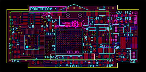
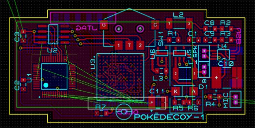
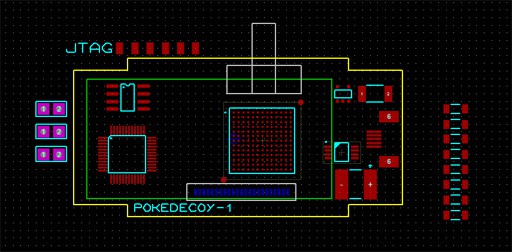
I want to use a CPLD to get as close as possible to the original Gameboy Pokemon sounds, by trying to copy the Gameboy's APU logic.

I chose one from the newest MAX 10 range from Altera, which really are cheap FPGAs with embedded flash. I had no choice but to go for a 0.8mm pitch BGA package.

The CPLD only has a clock input, mixed parallel/serial input bus, and one PWM output.

Pokemon pictures and cry data directly copied from the Pokemon Crystal ROM are stored in a 1MB SPI flash chip, which a LPC1342 ARM microcontroller pulls when requested to display on the OLED display and feed as APU registers updates to the CPLD.

The high frequency PWM audio is filtered by a R-L-C network and then amplified by a SSM2305 class D amp for a small 8-ohm speaker.

An electret microphone allows for simple blowing detection (noise amplitude), and a two-way navigation switch allows for Pokemon selection.

The whole thing is powered off a single cell LiPo battery, which is charged by USB.

  • 1 × ABS-221-RC Speaker
  • 1 × SSM2305 Class D audio amp
  • 1 × MCPL3-AC-V Navigation switch
  • 1 × S25FL208K0RMF 1MB SPI flash
  • 1 × LM3671MF Buck converter, battery to 3.3V

View all 8 components

  • Layout (virtually) done

    Furrtek11/17/2015 at 05:13 0 comments

    I don't regret going for 0805 passives instead of 1206.
    Everything fits, there are only 6 components on the back right-hand side to save a millimeter when the board will be pressed against the battery.

    I can't get DXF import to work correctly in Solidworks so I'm just taking the biggest tantalum cap as height bound.

    I followed Altera's recommendations for the CPLD's connections, but I'll still be in doubt until I get the "Programming succeeded" message.

    Next step is to order the components and check their footprints. Then GERBER check and it's off to PCBCart for a week. I'll try to R-E Pokemon Crystal's sound engine (or part of it) while waiting.

    No updates on the enclosure, waiting to have a functional board before ordering the prints.

  • Layout progress

    Furrtek11/12/2015 at 14:13 0 comments

    Yesterday, I noticed (too late again) that OSH Park couldn't handle the trace width required for the CPLD routing. As I didn't want to have both special trace width and inner-layer requirements, I'm trying to keep the board only 2-layers to go for PCBCart's prototype service.

    They do 4mil/4mil traces and 13mil vias for a reasonable price.

    SPI flash, JTAG, switch, power supplies, and audio section are done.

  • CPLD and more component selection

    Furrtek11/10/2015 at 21:13 0 comments

    Component selection should be final now, the power supply part was missing.
    The battery charger, 3.3V step-down, and 5V step-up for the audio amp are chosen.

    Regarding the CPLD itself, I realized earlier today that the GB APU would never fit in 160 blocks. So I went towards FPGAs. Expensive FPGAs. Which need 3 different power supplies, flash,...

    I was ready to go for a $25 Spartan3A and say goodbye to board space and battery life when @Gozilu reminded me of the new MAX 10 series from Altera !

    I usually refrain from using new products because of fear or complexity, but those seem perfect for this application: 2K LE CPLD with 13kB of BRAM and sleep mode for $8 ? YES PLEASE !

    Here's the board outline with all the main components footprints.
    The CPLD is a 0.8mm pitch BGA, less scary than the BGA36 version of it, at 0.5mm. A waste of I/Os but it doesn't matter.

    CPU and memory are on the left, power supply and audio on the right. Display pads on the back (blue).

  • First update, mostly mechanical

    Furrtek11/10/2015 at 10:25 0 comments

    Just found out I could use Hackaday.io instead of my messy website.

    Here's what is done:

    • Main components selection
    • Most of the case's design, as seen in the project picture
    • Parts fitting in case

    And what has to be done:

    • Print case design for checking
    • Draw schematic
    • Draw board layout (shape export from Solidworks done)
    • Fully undestrand how Pokemon pictures are compressed in the GameBoy ROM
    • Fully understand how Pokemon cries are coded and played in the ROM also
    • Write firmware

View all 4 project logs

Enjoy this project?

Share

Discussions

Similar Projects

Does this project spark your interest?

Become a member to follow this project and never miss any updates