 Blair Vidakovich
Introduction
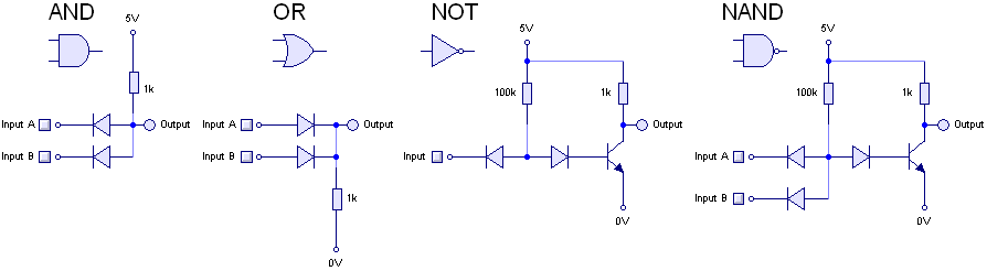
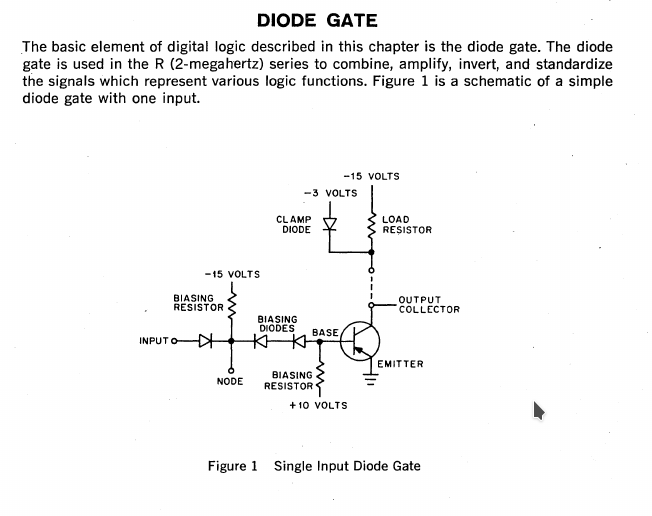
Hello! This is Blair Vidakovich. I was recently given entry into the hackaday TTLers group! I have tried many times, unsuccessfully, to create a discrete component computer. My basic logic element was a NAND gate, and I was using a popular form of DTL logic unit. I was copying the same electronic schematic as the Tiny Tim DTL computer. You can find the research and build log for this abandoned project here: (http://www.northdownfarm.co.uk/rory/tim/tinytim.htm). Anyway this was my basic logic element, the NAND on the far right.
I got stuck trying to build a ring counter, which I suppose I would use for control signals. I now see that a ring counter was not necessary, because many TTLers have gotten away with functioning discrete component computers without ring counters. In fact many people have successfully built four-phase clocks, so I now don't really need to worry at all, because the problem has been solved for me!
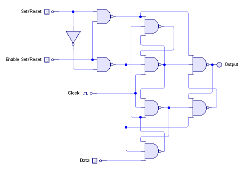
The reason why I got stuck was because I was attempting to build a DTL edge-triggered D flip-flop, and no matter how I tried, I could not build one that contained SET and RESET terminals. I could build one with just a clock and an INPUT terminal, but I could not go any further:
Enter the Discrete-Component PDP-8
I started researching and building a discrete component CPU/computer when I was diagnosed with schizophrenia in July 2013. The level of detail and concentration you have to come to master prevented me from getting any more delusional. I gave up the project when I started my PhD in 2015. I made another attempt to make a four-phase clock in 2016, but I failed again.
Then when I returned to this project a month ago (Feb 2018), I remembered I came across some schematics for an old discrete-component IBM computer back in 2013, but balked at the idea of using their basic logic element because it used so many bizarre voltages. "It used negative voltages!" I thought. There was no way I was going to be able to manage a project with such whacky logic levels, like negative voltages for positive logic signals. I went down the TTL logic route for five years.
This time, in 2018, I was determined to get further. I knew discrete component computers were built in the 50s and 60s, and I knew they were able to generate clock signals and have multi-phase clocks. All I had to do was find their schematics.
So I did. I found a wealth of resources on the DEC PDP-8. It is a wonderful computer architecture. It has a single accumulator you use with something like 6502 zero-page memory addressing in order to perform calculations. It is very RISC-like with a tiny number of opcodes, and it only contains something like 500-odd gates. So in February I thought it would be a wonderful computer to clone.
...if only I had enough money.
When I found out I could join this TTLers group, I decided I wanted to share my research on the strange DTL architecture of the PDP-8 in the hope it would help somebody.
The Standard Logic Pulse of the PDP-8
Before I start describing the electrical and logical system of the PDP-8, I want to explain how I came to obtain all this information. I retrieved it from pdp8online.org. Virtually the entire library of information required in order to repair, construct or just simply understand the PDP-8, as well as other DEC minicomputers, is all online at that website.
All of the information I have explained here comes from the DEC 1967 Digital Logic Handbook. It is the last digital logic handbook that uses R-series logic. From 1968 onwards, DEC uses M-series logic, which is basically just normal TTL.
Anyway here is the standard logic pulse of the PDP-8.
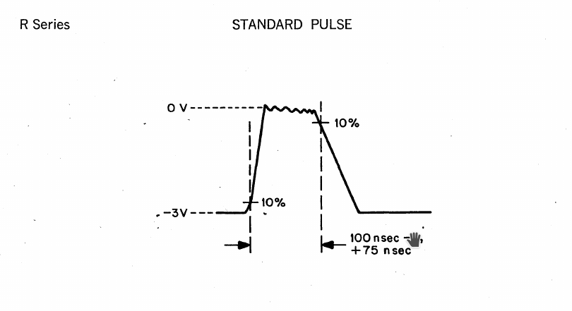
The PDP-8 uses DEC's proprietary R-series logic. As the following diagrams explain, R-series logic takes a -3V signal to be a digital ONE, and a 0V electrical signal to be a digital 0. This is very whacky, and may seem strange, but there's nothing theoretically incorrect about using negative voltages in one's logic system. Virtually any voltage differential can map onto whatever number system you want your computer to use. By the time we get to Diode-Capacitor-Diode gates, the reasoning for -3V = 1 will become apparent.
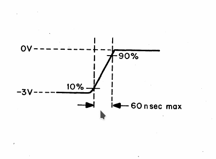
This diagram explains the standard rise and fall time requirements of standard logic pulses in R-series logic:
The Standard DEC Logic Gate Symbols
So that the later diagrams and schematics make sense, it is important to understand the symbols for different logic elements that DEC employed in order to describe the R-series logic system. Here is the explanation:
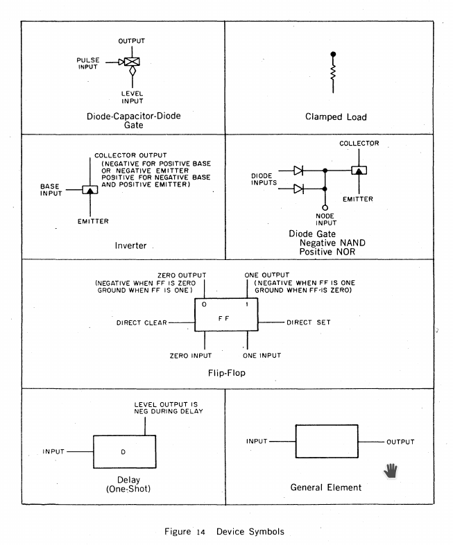
Here, in Figure 14, we can see (from left to right, down the page) the symbols for Diode-Capacitor-Diode gates (DCD gates), for a PNP transistor, for NAND and NOR gates, for RS flip-flops, for monostable multivibrators, and for general logic functions.
R-Series Logic Signal Symbols
The R-Series logic construction of the PDP-8 doesn't just use standard -3V signals for digital ONEs. It also uses positive logic PULSES, in addition to LEVEL logic signals (in order to edge-trigger flip-flops), and it uses negative PULSES, as well as non-standard signals where it isn't possible to efficiently construct logical elements electrically using standard signals and pulses.
Please find the standard DEC R-series logic signal symbols below.
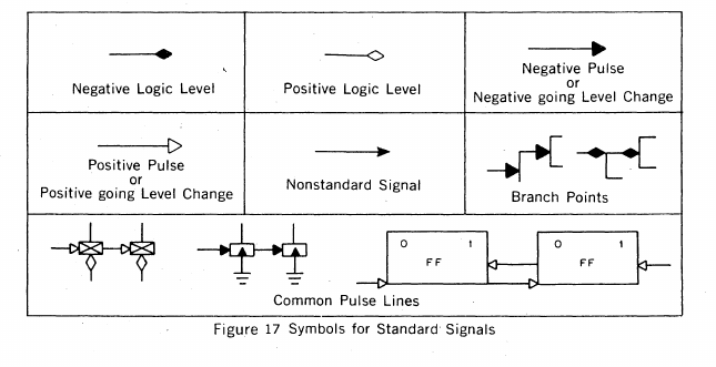 You can see why I originally dismissed this system in 2013, because it can seem theoretically unparsimonious. It is very promiscuous with its conceptual implementation, BUT, as I now understand, this is for the purpose of making R-series logic computers very easy to construct by hand. This allows the PDP-8 to be constructed with the minimal number of electronic components, and it simplifies the overall electrical schematics.
As you can see, the DCD gates in the bottom part of the diagram are receiving positive logic level signals, and are triggered by positive pulses, and inverters are shown to be receiving negative pulses, or negative-going logical level changes.
The R-Series Logic NOT-gate
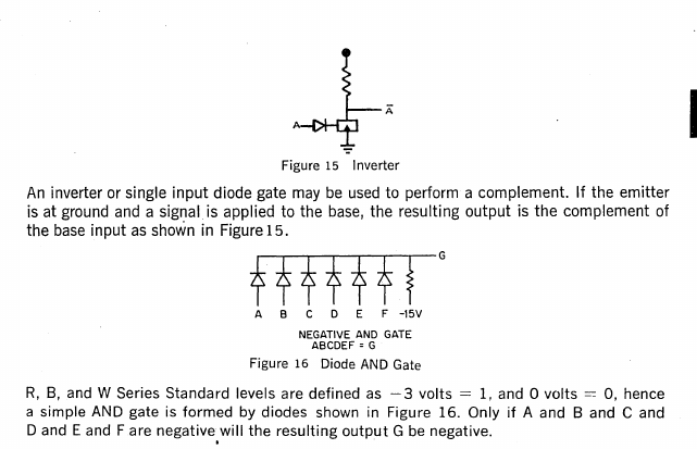
This is the standard inverter of R-series logic. Virtually every other passive logic element is constructed out of this gate:
It uses a PNP transistor, the exact electrical component equivalents I have found, and it uses far more diodes than in other DTL electronics. In fact, you'll find, when looking at the schematics of the R series flip chips, which I can provide, most of the logic is actually carried out by diodes, with signal voltages to be amplified later by transistors. Very few transistors indeed are used in R-series logic. This may actually be an advantage to the system.
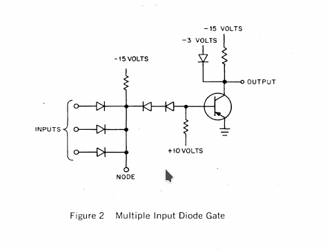
Figure 2 above shows what a multiple input diode gate looks like in R-series logic. With negative signals, this gate operates as a NAND, and with positive signals, it acts as a NOR.
Edge-Triggering: Enter the Diode-Capacitor-Diode Gate
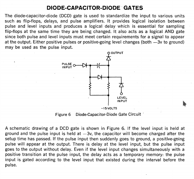
The diagram above explains the operation of the DCD gate in a sufficient level of detail. Pulses with shorter levels than normal logical pulses trigger the DCD gate, and using DCD gates allow one to be able to sample flip-flops while they are about to be changed. ADDING capacitance to a logical circuit seems like a crazy thing to do, but that is what DEC did.
DCD gates are a fairly clever solution to isolating logical inputs and outputs, as well as allowing edge-triggering. Edge-triggering using whole NAND or NOR gates can lead to many many semiconductor components being involved. Remember, using whole NAND gates transforms an logical-level D flip-flop from this:

to an edge-triggered d flip-flop, this:
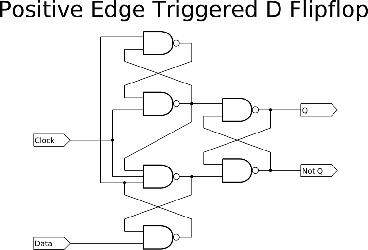
Not only do we now have one more gate, but we also have gates with multiple inputs, requiring more diodes. Nevermind that we haven't dealt with settable and resettable edge-triggered D flip-flops.
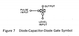
This is the symbol for a DCD gate. As you can see, they operate with POSITIVE logic pulses, and POSITIVE logic level inputs.
Flip-Flops
In much the same way as DCD gates allow input-output isolation, and edge triggering with few electronic components, DEC standard RS flip-flops are also very simple in their electrical construction. They use few components, and would therefore reduce the overall size of the PDP-8, as well as its operating power, and heat footprint. The R-series logic RS flip-flop below reminds one of a simple RTL flip-flop.
You can also see the logical symbol for the standard R-series logic flip-flop below.
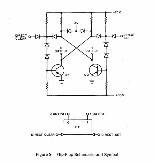 RS flip-flops are almost always combined with DCD gates, which allow the logic element to perform in dynamic operation. Outputs may be sampled as inputs are waiting to be transferred into the logic element, so DCD gates allow logical isolation.
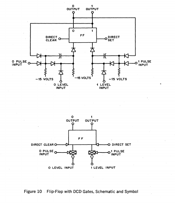
As you can see, flip-flops require POSITIVE logic level singals, and POSITIVE logic pulses.
Complementing Flip-Flops
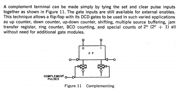
The power of the DCD gate is apparent here - without any extra components, a normal RS flip-flop can be turned into a complementing JK flip-flop.
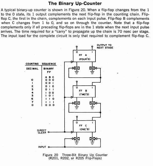
Complex Logical Elements
This is a very quick example of how R-series logic flip-flops would be combined into a complex logical element. There are a great many examples in the R-series logic handbook, like settable and resettable counters, etc.
The Legacy of RTL in R-series Logic: Pulse Amplifiers
Because most of the logic calculation in R-series logic is performed by diodes, R-series logic requires analogue electronic elements. The fan-out of digital logic elements is limited, so amplifiers are needed to restore electrical signals to their proper voltage and current rating. All of the standard fan-out capabilities of standard R-series logic flip-flops are in the 1967 Digital Logic handbook, if you're looking for more information.
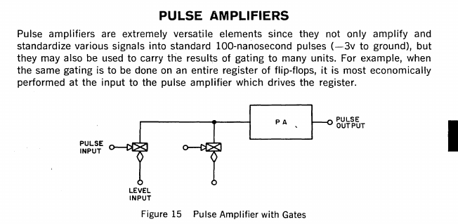
This is an example of a flip-chip module which is a pulse amplifier, the R601 module:
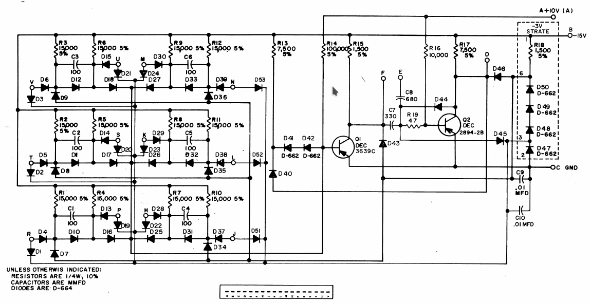
As you can probably gather, it is just 6 DCD gates combined with a transistor amplifier.
Component Substitution
When you look at the R-series flip-chip modules, you're probably going to end up despairing because many of the components used in the modules are now obsolete. I have done my best to scour digikey and mouser to find as close electrical equivalent components for all the major elements of the flip chip modules.
That said, if this does present itself to some people as an attractive electronic logic system, we may just reconstruct all the basic logic elements using easily accessible components.
Webpage with original DEC substitution recommendations HERE: (http://so-much-stuff.com/pdp8/repair/subst.php)
| Original DEC Component | DEC-Specified Component Substitution | My Suggested Substitution |
| D-662 Diode (High Forward Voltage Drop) | 1N645 | 1N4004 |
| D-664 Diode (Low Forward Voltage Drop) | 1N3606 | SB140 Schottky Diode |
| DEC-3639 PNP Transistor | 2N3639 | 2N4403 |
| DEC-3009 NPN Transistor | 2N3009 | BC559/BC549 |
| DC-2894 PNP Transistor | NONE (!!) | 2N4403 (?) |
Conclusion
If you found any of this useful, please check out my blog at https://bootlicker.party/
Discussions
Become a Hackaday.io Member
Create an account to leave a comment. Already have an account? Log In.
I am going to have to check this out much deeper. Your basic DTL Nand is what I use as my basic logic gate for my IO build and what you present will help me a lot :-)
Are you sure? yes | no
Let me know if you'd like all the schematics - I have them all.
Are you sure? yes | no
That would be great. I started on this DTL/TTL adventure almost two years ago not knowing anything about it and just learning by doing and information found here on the internet :-)
Are you sure? yes | no
awesome. i think i may upload the documents to the TTLers group, actually
Are you sure? yes | no
Wow ! This is a fascinating explanation ! I had never heard about the DCD but in the context of a Flip-Flop, it now makes sense because it's one element of a circuit that puzzled me in the past...
When do you start building your own PDP8 clone ? :-)
Are you sure? yes | no