 Yann Guidon / YGDES
I'm already back with another ring oscillator ! and @Tim will love this one even more.
The precedent one gave me some headaches due to the bad PCB design, I used a single-sided board and couldn't solder anything on the other side... ma que stupido !
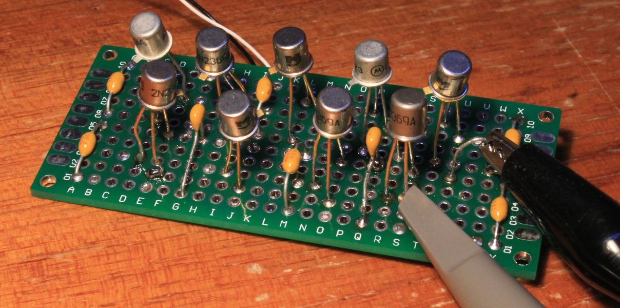
I de-soldered the transistors and made a new board with more headroom. Aaaaaand...
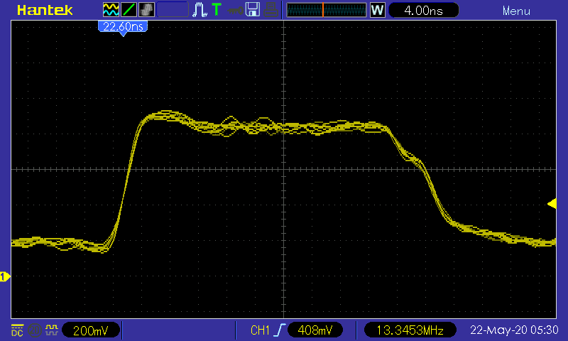
13.30MHz @ 2.42V / 30mA => that's 4.2ns per inverter !

The new parameters are not far from the previous one :
Rb = 150 Ohms, Rc = 470 Ohms
The change of Rb seems to have helped a bit : I now see the collector voltage saturated and not reaching Vcc (between 0.15 and 1.25V). Vb ranges from 0.18V to 0.9V => I'm now near the levels defined by CDC !
.
Here is the waveform at the base : the 2N2369 is driven hard at 800mV ! Discharging it however seems to take some time...
The other change is the ample decoupling, 6×100nF + 3×10nF, I don't know if it helps but you're never too safe with that because later, I might unexpectedly scramble the local CB channels ;-)
Yet I don't see how/why I gained 30% speed with the same transistors (I replaced one by error) and almost the same resistors (ok the base resistor has lost 25% of its value... but it's worth it right ?)
Did I mistake a resistor somewhere ? Was one of the transistors "too slow" ? Is there a wrong resistor value in the first RingO ?
Something else is interesting : I'm now at 30mA but the last "record" was at held at 50mA so something serious is going on here ! Efficiency has jumped too !
The signal falls in about 5ns on the 200MHz scope, which is close to the limits. There is some overshoot, very likely caused by the ground clip and the limited BW of the whole system.
Another good sign is that the falling edge (at the collector) is now the fast one, in 5ns :-) (we were puzzled that the rising edge was the fast one on the other board, might have been mistaken for the base ? nah...)
The rising edge takes about 12 ns to completely reach 1.1V and this will get only longer with more loading. But in 8ns, 1V is reached.
At 2.5V and 470 ohms shorted in DC to 0V, the collector current is drawing 5mA (approx.)
Add to this the other current source (the base capacitance and the transistor might have 10mA transients... So once again it's in line with the CDC specs :-)
The base current is defined by (Vc - Vb) / Rb = (1.2 - 0.85) / 150 => Ib = 2.3mA (at 2.5V, during DC ON) => in line with the expected values :-)
The circuit alternates between 5mA and 2.5mA, this averages to 3.7mA/9.3mW per inverter (FO1).
The delay :
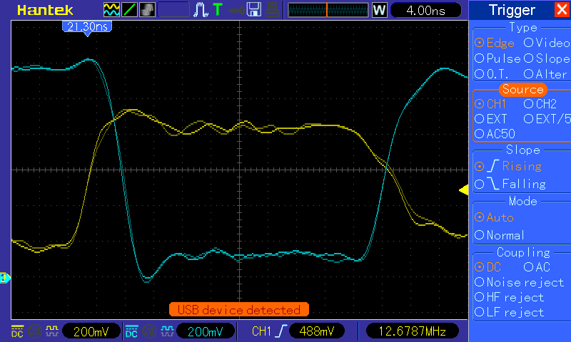
This plot is from the base and collector of the same transistor, so we see the latency of the signal : about 5ns between the middle point of the rising edge on the base and the middle point of the falling edge of the collector. It takes about 8ns from the start of the base's rising edge to the end of the collector's falling edge...
The reverse however takes more time, due to RC loading.
The V/F curve :
V     mA   MHz
1      6   8.292
1.1    8   9.191
1.2   10   9.942
1.3   11  10.576
1.4   13  11.140
1.5   15  11.609
1.6   16  12.001
1.7   18  12.344
1.8   19  12.636
1.9   21  12.867
2     23  13.053
2.1   24  13.182
2.2   26  13.286
2.3   28  13.343
2.4   30  13.364
2.5   31  13.354
2.6   32  13.317
2.7   34  13.253
2.8   36  13.170
2.9   38  13.068
3     40  12.952
3.1   41  12.826
3.2   42  12.689
3.3   44  12.552
3.4   46  12.408
3.5   48  12.253
3.6   49  12.097
3.7   51  11.938
3.8   53  11.729
3.9   55  11.580
4     56  11.426
Clearly : something important has happened :
set xlabel 'V'
set ylabel 'MHz'
set y2label 'mA'
set xr [1:4]
set yr [6:18]
set y2r [0:120]
set ytics 1
set y2tics 10
set key right bottom
plot "27pf.dat" using 1:3 title "v.1 27pF Frequency in MHz" w points pt 7,  \
     "27pf.dat" using 1:2 axes x1y2 title "v.1 27pF total current in mA" w points pt 7,  \
     "ringo9_2_sans.txt" using 1:3 title "v.2 sans cap Frequency in MHz" w lines, \
     "ringo9_2_sans.txt" using 1:2 axes x1y2 title "V.2 sans cap current in mA" w lines
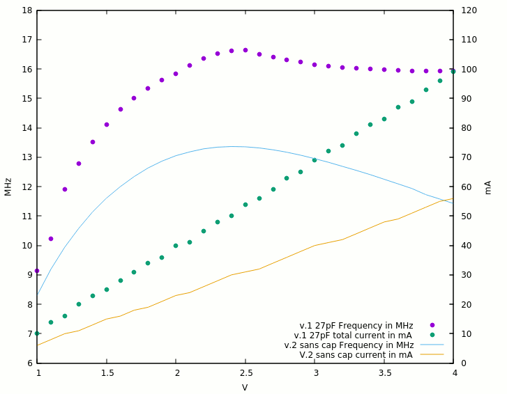
The behaviour is temperature-sensitive...
The PSU's ammeter is really wiggly !
Efficiency at peak (2.5V) :
- v1+27pf : 54mA 16.65MHz 135mW => 8.108mW/MHz
- v2 : 31mA 13.354MHz 77.5mW => 5.8mW/MHz
Something really interesting is happening since v1 ! Is it thanks to all the decoupling ?
Discussions
Become a Hackaday.io Member
Create an account to leave a comment. Already have an account? Log In.
@Tim Could you re-test your prototype with ample decoupling, spread all over the board ? A bunch of 100nF might make a significant difference !
Are you sure? yes | no
I am not in my home-office right now, so I can't look into this. Will follow up sometime next week.
Pretty interesting results! In my ring-oscillators I left the decoupling cap unpopulated. Will try to see what happens when I add it. I suppose it could affect the slew rate, which should have a big impact especially with reach-through-cap.
Btw, at some point also ESR of the caps should play a role. Could this explain some of the weirder stuff?
Are you sure? yes | no
Hi !
I'm curious to see what will happen. Apparently 100nF per pair of inverters would do significantly positive effect. Or maybe one 47nF per inverter to reduce ESR.
I have no idea what was so weird between v1 and v2. The decoupling is the major difference, I have put 5×100nF and some lower values... The layout too has changed, with the ground at the middle, but I don't see why that would affect the circuit at this point. The transistors are the same, the Rc is the same.
Rb=150 seems to be "right". And I was thinking : that's a CLEVER TRICK because there is less need for a Baker clamp.
On the contrary if the base exceeds 0.2V+Vf of the schottky diode, the transistor would be limited to 0.5 or 0.6, which will not fully saturate the transistor and the VceSat would not go down to 0.2 or less. The 2N2369 is specifically designed for this operating mode... The base cap would help though, with or without diode.
Look at the next log (in construction) for the latest finds !
Are you sure? yes | no
Ok, I did look into the effect of adding a decoupling cap now. I had previously left all the pads for the decoupling pads unpopulated so I added a single 100nF cap to my oscillator with 470/150/68p. Turns out there was no effect at all, so this does not seem to play a role.
No idea why you observe differently? My RINGOs are all built up on a custom PCB with SMD components and a pretty dense layout. Maybe this already reduces parasitics to a level where it does not matter?
Are you sure? yes | no
That's so...
odd.
Maybe I replaced one transistor that was really slow... I binned for hFE and one of them was suspected with NC base. It might have been a "sour lemon".
Are you sure? yes | no