 Yann Guidon / YGDES
I found the original source of that story (ECL or CTL : what's the fastest topology for discrete gates ? [updated]) about "CTL" (Complementary Transistor Logic, which, since it doesn't invert, can't qualify as logic :-P ) http://www.6502.org/users/dieter/mt15a/mt15a_3.htm
The author presents his TTL gate, then his modification inspired from TTL.
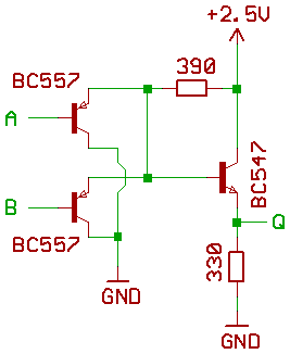
I did some tests and tried a basic gate and... "it's a weird AND".
More precisely it works as a linear amplifier with close to no voltage gain but strong current gain. When the circuit is rewritten, it's obviously a pair of complementary "emitter followers" with the output clamped above 2.5V-Vbe=1.7V. The output can go down to about 0.2V on my tests.
This circuit also has a strong tendency to oscillate. My test setup was poorly designed but I could stop 60MHz oscillations with a 4n7F capacitor at the input of the PNP. I'll see how I can get a stable circuit...
Since this is just a pair of emitter followers, why bother with using PNP inputs after all ? With my BC559C, each with hFE=480, the overall gain is about 200K, the input current is very low but this is overkill and oscillations are not surprising at all.
The PNP emitter followers at the input are nice. The NPN emitter follower at the output is nice. AND gates are very useful in some places. However this is not what we expect from a "logic gate" because there is no real "active level" or "threshold". Current gain is nice but voltage gain is important too ! So this CTL might be faster than ECL but ECL can do more functions and provide inversion.
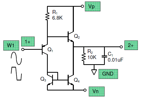
Furthermore, it looks quite a lot like the Low Offset Emitter Follower :
After this little setback (or disappointment) I looked at other ways to make this circuit and a variation appeared : it replaces selected PNP input transistors with NPN.
Thus instead of inverting the output, we can invert the necessary input(s) and we apply "bubble pushing" :-)
Of course the logic levels are modified but this leads to the interesting concept of a cascade of emitter followers, "or-dotted" together for the OR functions, with parallel transistors for AND or OR functions, and complementation (switching from PNP to NPN and vice versa) for the negation.
Of course we can also use BJT as ANDN gates :-)
Discussions
Become a Hackaday.io Member
Create an account to leave a comment. Already have an account? Log In.