 Yann Guidon / YGDES
The circuit has been updated but here are the original design elements. Read the comments for more details :-)
So here is the old schematic: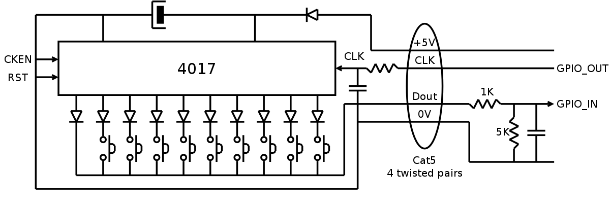
Requirements
Cheap. A CD4017 or 74HC4017 costs about 1$, add some "dust" (diodes, resistors) and a small PCB.
Simple and compact: yes too :-)
Low power: at most a few mA. (fail: the DC/DC draw much more, even unloaded)
Reliable: should be immune to EMI. Cat5 cable uses twisted pairs which should protect the signals over medium/long distances. A fluorescent lamp's ballast or other mains-conducted EMP could be picked up but should not disturb the system.
Easy to interface and program, with a robust algorithm that works even when the keypad is removed.
Wire-level Interface
The constraint is to read the buttons over existing Ethernel lines in a EMI-prone environment.
Many projects use a 74HC165 (for example this one  ) but this method requires at least 2 control signals: PL (load data) then CP (clock pulse to shift data).
With the 4017, only one control signal is necessary: clock. This makes the system inherently more reliable (one point of failure less). Synchronisation is achieved by using one of the output signals, which will always be "on" (think about a serial link with a start bit that is on).

The 4 twisted pairs are used, one of the wire in each pair is tied to a common 0V/GND. The others are:
- 5V
- Clock
- Dout
- 5V
The original version is not isolated since there should be no electrical contact with anything else in the remote circuit. I added it anyway...
The 4017's clock input must be well filtered because any undesired pulse on this line would break the synchronisation. A RC filter + Schmitt trigger is used so far. This is less critical on the controller's side because the data is sampled just before changing the clock level, which happens at a pretty low frequency.
5V vs 3.3V
(moot: the optoisolators now remove this concern)
The Raspberry Pi is a 3.3V system but the 4017 is powered by 5V. Here is the trick:
- The Ethernet cable has some inherent resistance that is proportional to its length. It should be about a few Ohms but it still counts.
- The power supply of the remote board goes through a PN diode, which drops about 0.6 to 0.7V. A capacitor smoothes the voltage.
- The 4017's pins have some inherent resistance too (resistance is futile but it's everywhere...)
- The Dout signal goes through a diode, which drops another 0.7V.
- At this point the voltage on a Dout signal can reach 5V-(2×0.6V)=3.6V. It is further reduced by a resistor network on the GPIO input: 1K Ohm in series and 5K of pull-down. The "on" signal is now around 3V.
A 100nF capacitor in parallel with the 5K pull-down will filter out some transients. As it is in series with the 1K resistor, the inrush current that charges it is limited.
For the 4017's clock input, the 5V supply wouldn't be usually compatible with the 3.3V GPIO signal. However, the margin is valid because of the diode drop: 5V-0.7V=4.3V, the Vih is usually 70% of Vcc, 4.3×0.7=3V, which is 10% lower than 3.3V.
Timing and algorithm
The keys are scanned at low speed, giving time to settle for all the electronics.
A polling routine is called at about 100Hz. This drives the clock output signal, so half the calls are just about changing the clock signal (there are 2 edges per cycle).
The other edge runs a software finite state machine, driving the synchronous bitstream, which works in either of two modes: scan or synchronisation.
- Scan is the "normal" operating mode. The sync bit arrives at the expected moment (every 10 cycles) and the rest of the bits show which buttons are pressed.
- If the remote is unplugged or being powered up (the filtering capacitor does not load immediately and the 4017 can be badly initialised) then the sync bit is not regular and the controller sends pulses until it is regular again.
Internal counters are incremented until a button is considered pressed or until the bitstream is in sync. 3 consecutive identical valid frames are considered as givin "valid" data.
Logs:
1. Isolation
2. First signals
3. Implementation
4. Last notes