 Patrick Van Oosterwijck
I find laying out boards too much fun. It's like a giant puzzle that slowly comes together, with difficult conflicting constraints but also freedom to find creative solutions. You start with a concept and a giant mess of parts and slowly it crystallizes into a beautiful reality. I think I'm addicted to laying out boards. ;)
Anyway, while I should be spending most of my time writing documentation and finishing the test fixture for the #LiFePO4wered/Pi+, instead I've been working on figuring out the floor plan puzzle for the wESP32 instead. And of course, you need to actually lay some parts out to determine if it will work. Here is the result so far (work in progress):
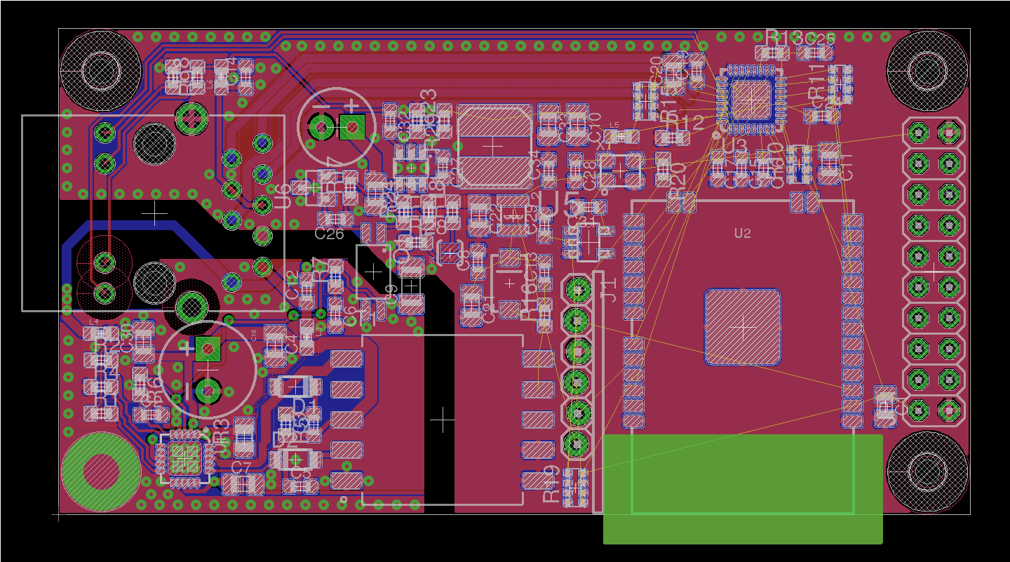
The hardest part was the isolated power section in the lower left corner. The layout of this part is critical to minimize EMI. It was also going to determine the width of the board. My goal was to make it 40 mm wide, but with the mounting holes and Ethernet jack taking up a good amount of space, this circuitry threatened to push the flyback transformer too far out, making the board longer and ending up with unused space in the middle.
Another difficulty was that I wanted the chip close to the mounting hole, which has metal throughout, so it can be thermally connected to a heat sink if necessary. With the "other PoE project" I have prototypes for, I had found that the design just barely supported 13W--with more load, the chip would go into thermal shutdown because the copper of the isolated area was barely enough to sink the heat away. Although I intend to use 2oz copper for this board, I still expect that I'll have more heat trouble at high loads because it's even smaller, and the isolated copper area is smaller as well.
To make things more difficult, PoE PD chips have an internal switch that keeps most of the power system disconnected while the PoE SE figures out the power requirements, and the bulk of the isolated "ground" area you see is not what's connected to the chip's thermal pad. No physical metal connection between the thermal pad and most of the copper plane in the isolated area will make it even more likely that heat sinking may be necessary.
I eventually found a solution by squeezing as much power circuitry as made sense through the gap between the Ethernet jack and flyback transformer and pulling the flyback as much to the left as possible. Then everything started falling into place.
The other big question was where to locate the Ethernet phy. Since the Ethernet jack is on the left and the ESP32 on the right, some connections were going to have to span the distance: either the TX/RX pairs or the MAC signals. Since the TX/RX pairs are 4 lines and the MAC signals 7, the choice was simple. In the screenshot you can see the phy right by the ESP32 and the TX/RC pairs routed as differential pairs with (hopefully) close to 100 ohm differential impedance.
This left the 3.3V buck converter located centrally close to both the phy and ESP32, which is great. I also succeeded in my goal to keep the tall components off to the left, while the right side only has low components so that plugging a board in that folds back over the ESP32 section (and partially even further) should be possible for nice compact systems.
I'm very happy with how this is coming together. I didn't even have to worry about removing any possibly "optional" footprints related to filtering and snubbers, which should give me all the knobs needed to optimize the power system's EMI performance.
For those who are curious, the current PCB size in the screenshot is 75mm x 40mm, and it looks like I should have no trouble finishing up the rest of the layout without having to expand it.
Discussions
Become a Hackaday.io Member
Create an account to leave a comment. Already have an account? Log In.