OSH VFD Watch
Open source vacuum fluorescent display watch.
Open source vacuum fluorescent display watch.
To make the experience fit your profile, pick a username and tell us what interests you.
We found and based on your interests.
VFD Watch V1.0(prototype) - Schematics.PDFSchematics for V1.0Adobe Portable Document Format - 1.34 MB - 03/21/2018 at 21:43 |
|
|
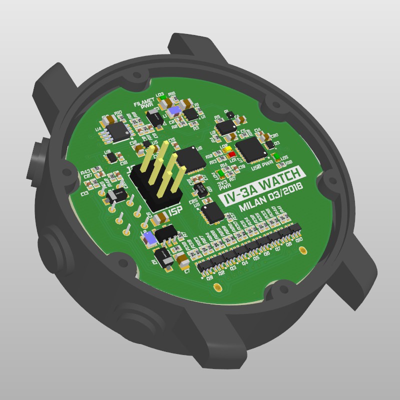
Here are some pictures of the watch assembly (I am only missing front glass cover). Back cover is made out of 1 mm thick aluminium. Transparent cover would also work so that the PCB can be seen (will tray that out). Case is printed with PLA 0.1 mm layer height. Watch is 15.5 mm in height and 50 mm in diameter and strap is 22 mm wide. As soon as I get some free time I will make video to show watch working and how it fits on the hand.
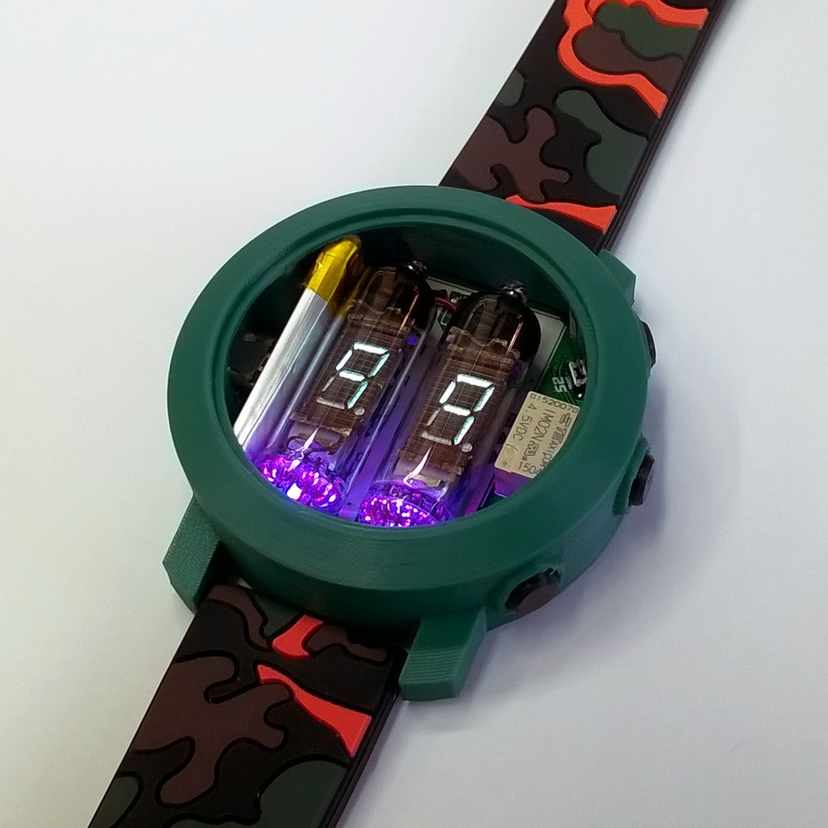 | 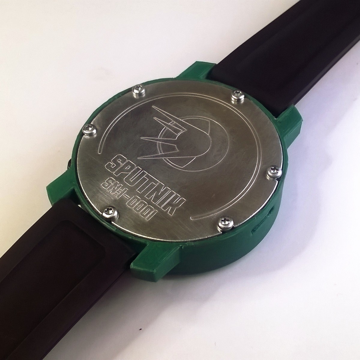 |
 |  |
This week batteries arrived. They are lithium polymer 4 x 10 x 30 mm with declared capacity of 110 mAh. First thing to do was to measure battery capacity in my application.
Procedure was to charge the battery up to 4.2 V and then discharge it with 45 mA (maximum current draw of the watch is 35 mA + some reserve) to 3 V. In Version 1.0 battery is not usable below 3.3 V, therefore I will drop 3.3 V rail to 3 V in the next version. Measured capacity was 86 mAh or 2 hours of active run time. With 30 min active time per day that would be autonomy of 4 days. I might add another battery, that would reduce current draw from single battery and get me maybe 100 mAh per battery. I think that should give autonomy of about 10 days.
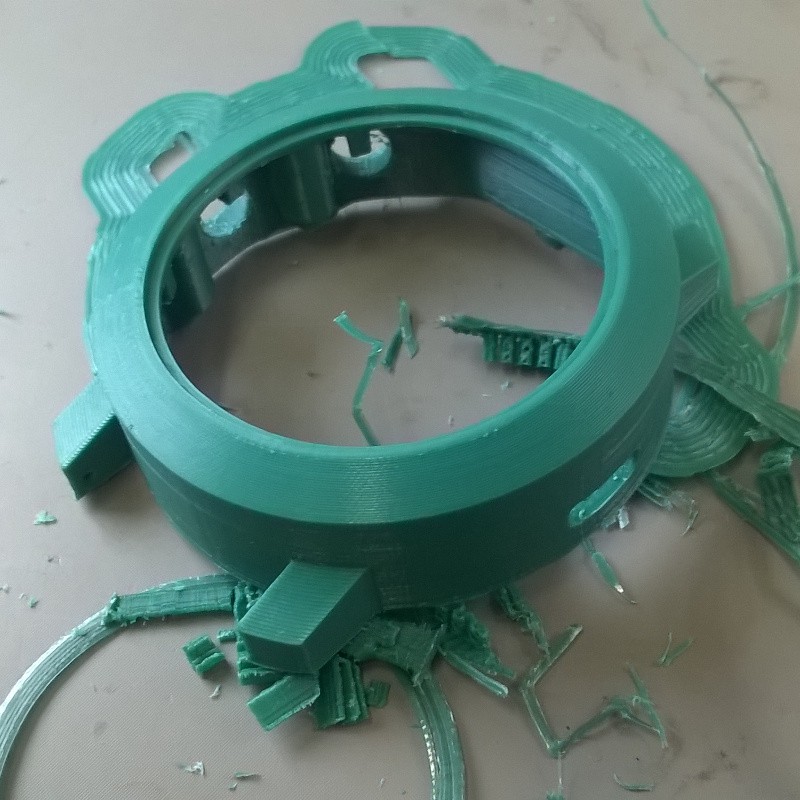
I also tried printing enclosure with PLA and 0.1 layer height. Enclosure turned out good but further tweaking and optimization is required. For now time required to print is 3 hours and supports are only needed for small indent for pcb and back cover what was not the case for first (not version shown in image).
Here in this video you can see progress I made so far. Also at the end working display can be seen.
As you can see I had to cut few traces and solder jumper wires to fix stuff i messed up. Stuff I changed:
1. Fix footprint of K1 (swap pins 1 and 8 on PCB)
2. Replace push-pull drivers with NPN switches (now anodes are switched on by negative logic)
3. Boost converter (U3) is still not stocked so I had to supply 20 V from my PSU.
All changes made to the PCB are documented in the Schematics (also available in .pdf check "FILES")
Next thing to do is to test RGB leds under the tubes and replace switches on the PCB (they aren't very good) because they broke. After that I will start printing enclosure and by then hopefully battery arrives so i can test fit whole assembly.
VFD is indication vacuum tube with three electrodes: Filament, Grid and Anodes. When supplied with voltage grid emits electrons. Depending on the polarity of supplied voltage grid accelerates or deflects those electrons preventing them from reaching anodes. When an anode is supplied with a positive voltage, it will attract the electrons which have been accelerated through the grid. Anodes are coated with phosphor which emits light when hit by the electrons.
For IV-3A tube datasheet values for Filament, Grid and Anode voltages are:
Filament - 0.85 ± 0.15 VAC
Grid - 15-30 V
Anodes - 15-30 V
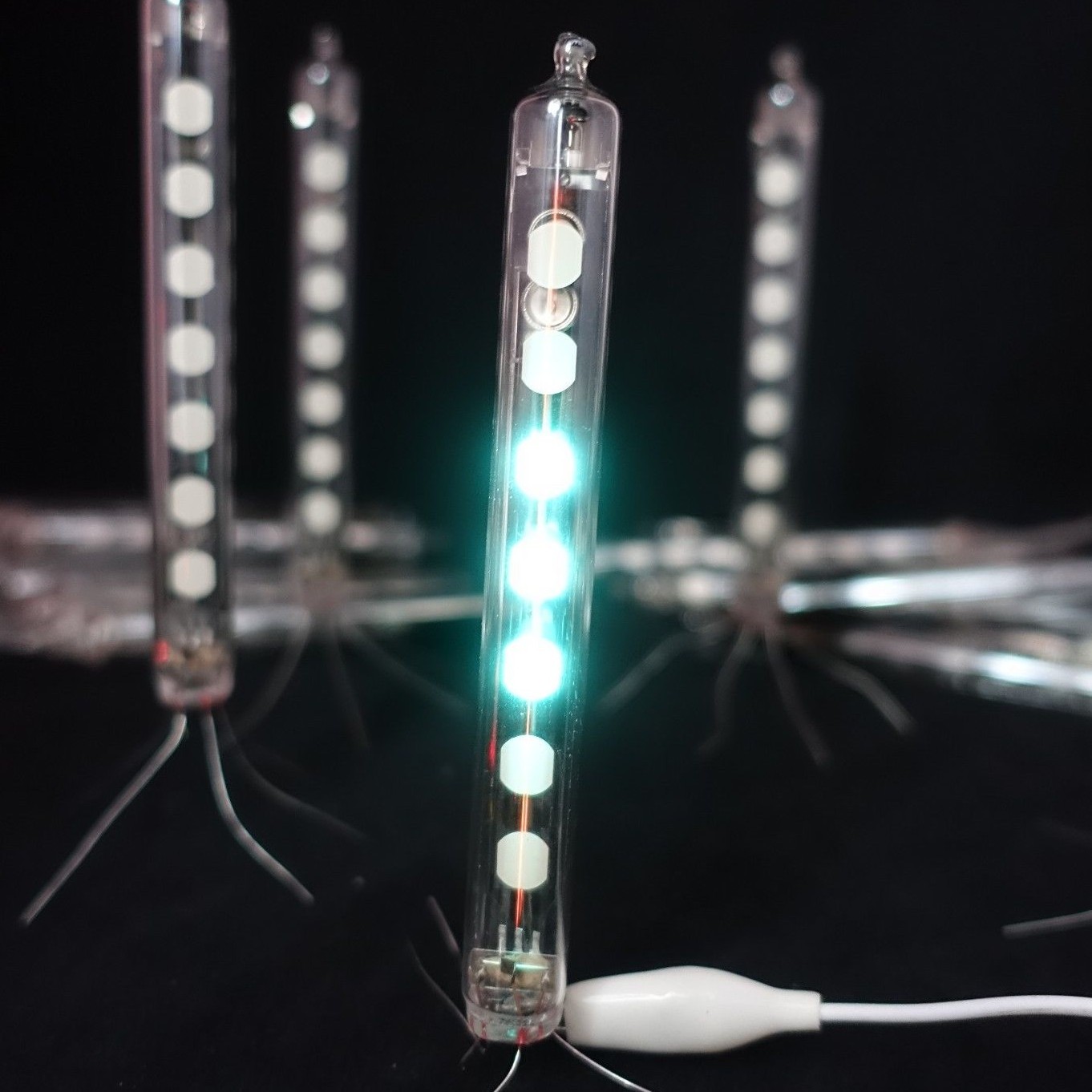
Generating grid and anode voltages is pretty straight forward by using boost converter or charge pump(depending on the required voltage and power source). Generating filament voltage on the other hand is a little more complicated. It is critical that the filament voltage is supplied within the specified ratings since the lifetime of a VFD affected by the extent of evaporation of oxide materials coated onto the tungsten filament wires.
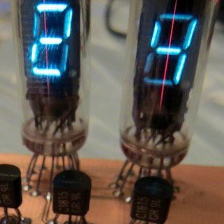
*Examples of overdriving filament (Notice thin red line).
 |  |
There are 3 ways to drive filament:
1. AC Filament Drive (50 or 60 Hz) - Most optimal method that uses transformer and mains power. Not applicable in watches :)
2. DC Filament Drive - Worst option. Introduces "luminance slant" - difference in luminance at opposite sides of the display due to the DC voltage drop. Effect is more apparent on larger displays than on single digit tubes.
3. Pulse Filament Drive (High Frequency RMS) - Most optimal method for my application. Use of astable multivibrator circuits for generating bipolar voltage pulses.
For generating filament drive voltage I am using LM4819 IC (mono bridged power amplifier - BTL amplifier). LM4819 consists of two amplifiers, one with unstable feedback loop (oscillator) whose output is feed into inverting input of second amplifier. Load is connected between the outputs of two amplifiers therefore the name for this topology - Bridge tied load. Full schematics of the circuit will be posted when I get some time to organize them because now they look like dogs breakfast.
When configuring amplifier 1/2 duty factor should be set, and the peak to peak pulse wave form should be 1.5 times or less than the RMS value. A frequency range of 10 kHz to 200 kHz is recommended.
For the end picture that shows current sate of the watch (Will post full description of progress in future project log. For now there is not much going on just testing of the circuit).
Yes that is small relay :)
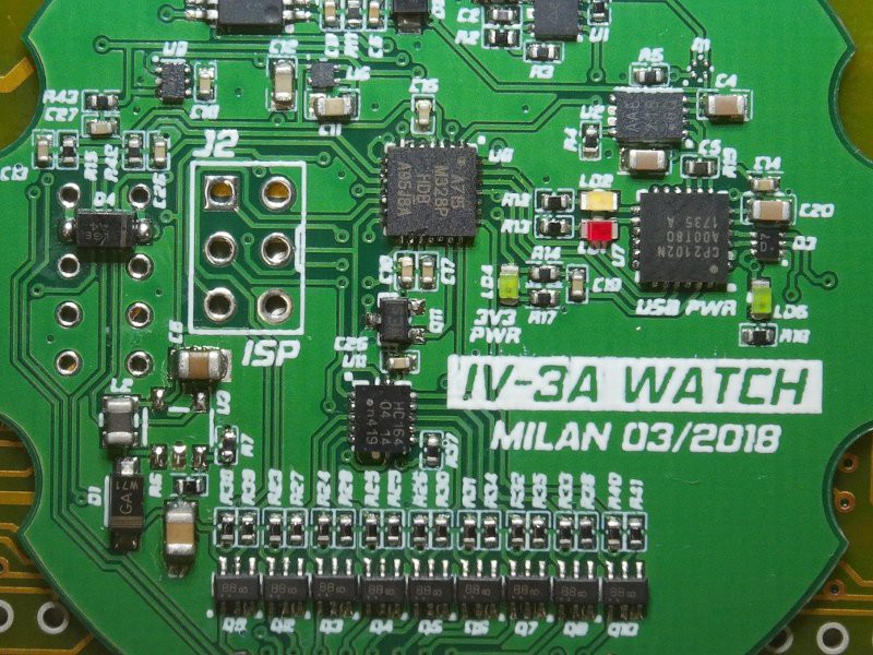
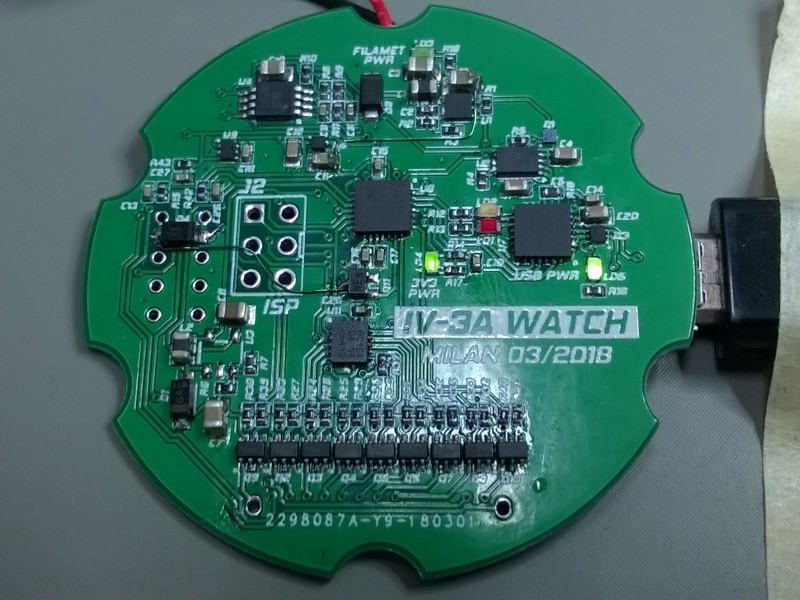
Today i finished assembling main PCB, although I am missing some non critical components. Next up is assembling PCB that holds VFD tubes and mounting the whole assembly together. Here are some pictures of the PCB giving firsts signs of life.
 |  |
And here are some pictures of tubes being used in project(I got bunch of them for cheap from Russia few weeks ago).
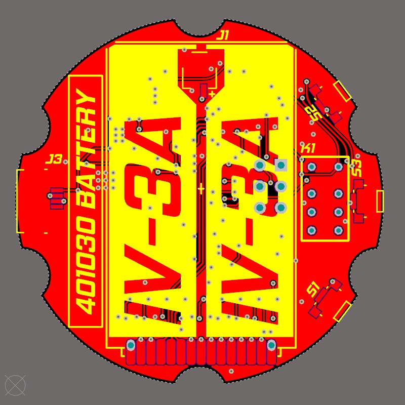
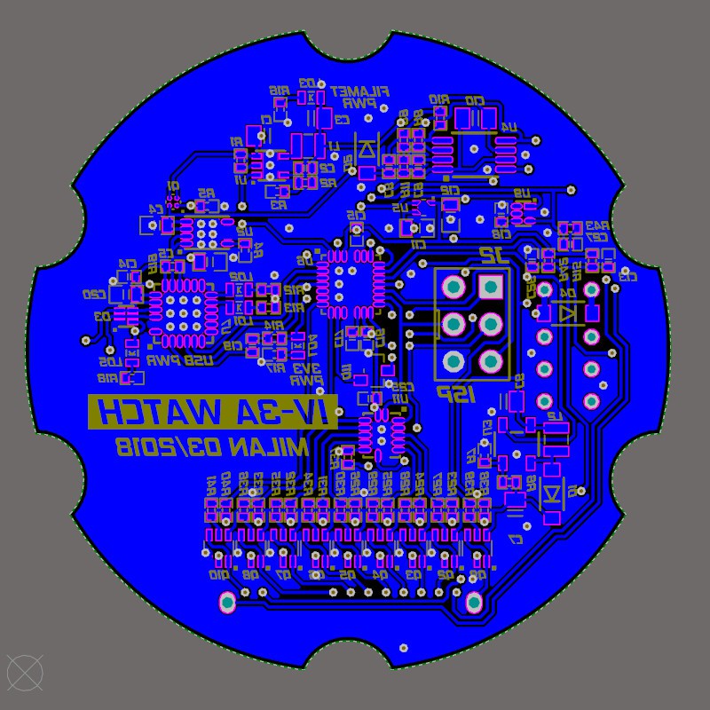
First prototype of main board is made on two layer PCB 44mm in diameter. Components used are mostly in SSOP, SOT and SOD packages. There are also components in QFN and 0402 packages which i plan to replace with QFP and 0603 eqivalents.
 |  |
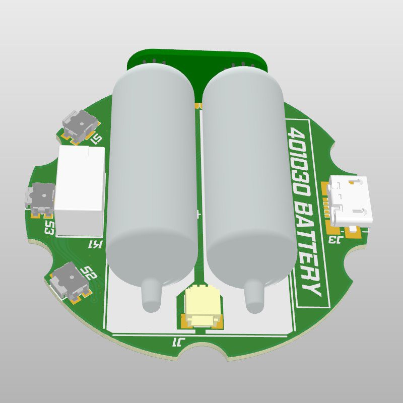 | 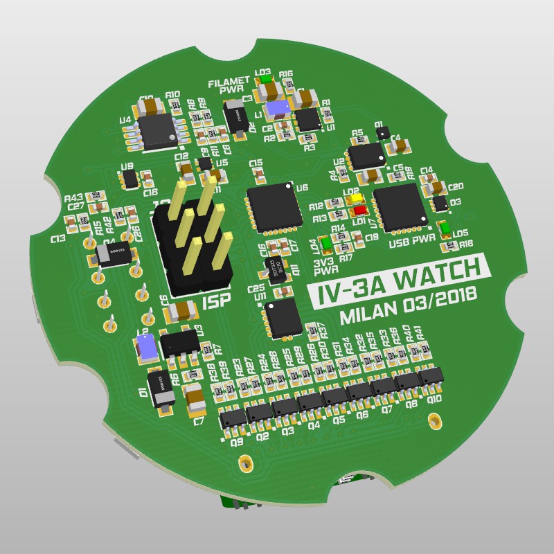 |
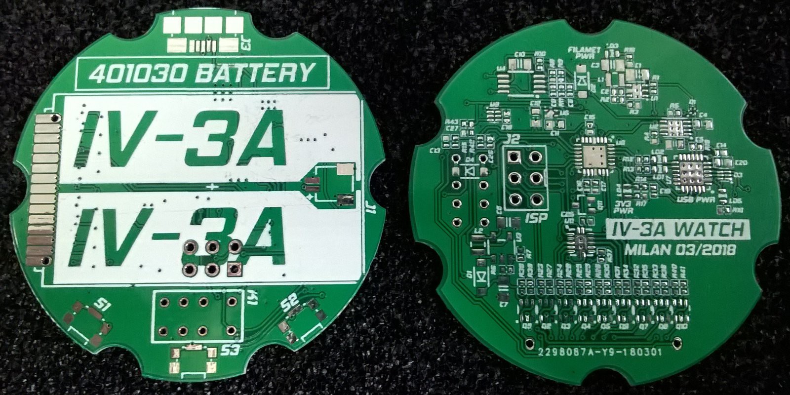
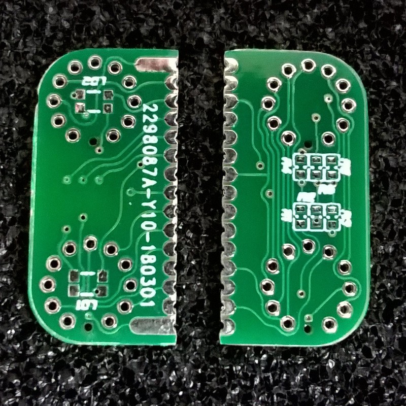
PCBs for this project were ordered from JLCPCB(that new-old PCB manufacturer every one is talking about). On first glance they look decent, but I will have to take a closer look once i have more time.
 |
 |
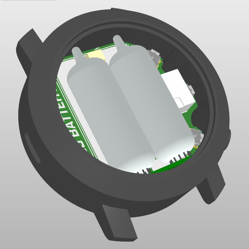
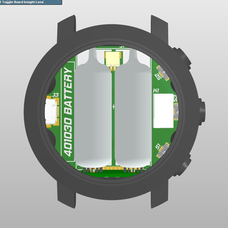
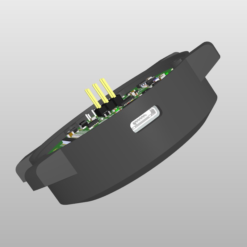
Enclosure is designed so it can be easily printed on inexpensive FDM printers. After I finish assembling and testing PCB will try to test print enclosure and post time-lapse video of print. Will try printing with ColorFabb PLA and nGen materials.
 |  |
 |  |
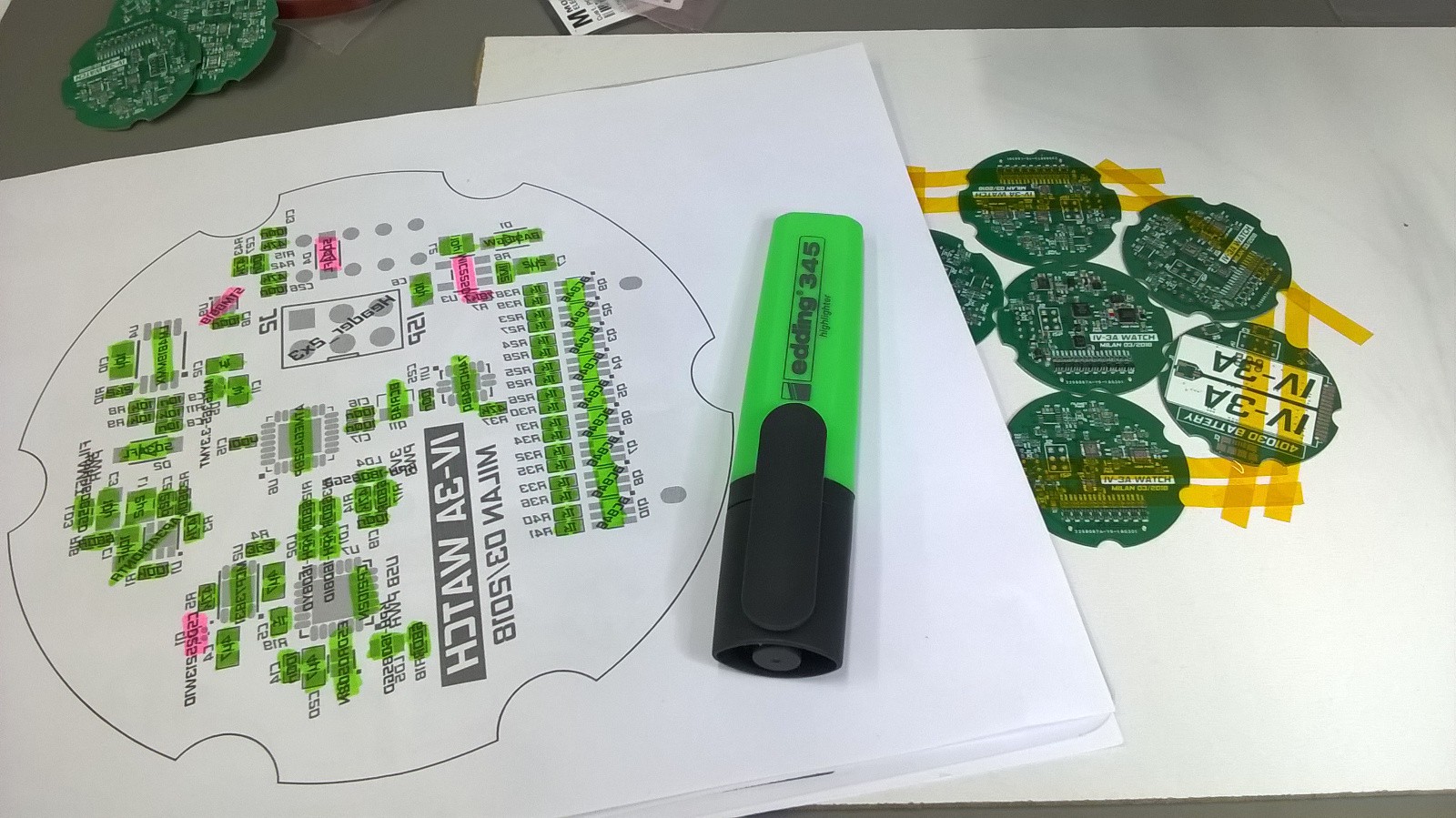
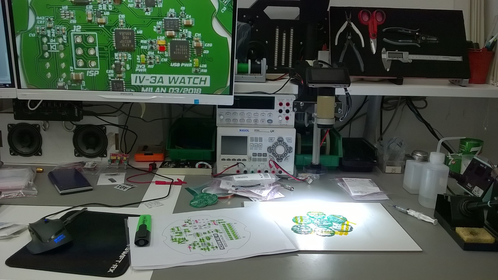
Some pictures of late night PCB assembly setup. Will post video of the complete process in a few days.
 |
 |
Create an account to leave a comment. Already have an account? Log In.
Nope, that's not me. That guy is doing nixie and vfd watches for some years now. I know him from instagram: https://www.instagram.com/guywmz/?hl=en
Hi Jacob. This project is not forgotten, I just had not had time to work on it :(. I hope I will find some this winter. Also got some ideas for new projects.
It become joke with my friends, always asking me when am I going to finish my projects.
Following your project closely.. looking forward to wear one soon! :)
Become a member to follow this project and never miss any updates
 Mile
Mile
 Stefan-Xp
 Adam Gulyas
 jaromir.sukuba
реле в качестве тикалки - гениально! попробую повторить проект. спасибо за схемы