 Nigel
NigelI was able to finish the analog module HDL as well as the digital simulator PCB. I’ll expand more on the latter tomorrow, but I’ll go over the ins and outs of the code used in the analog module in this update. The point of this module is to interface my chosen ADC on one end, and produce data and ram write requests on the other. This module in the end will be a few levels down from the top as we need to combine the data from disparate modules into a single address space that we can access from the XMega.
The analog module is comprised of 4 main parts, which I will cover individually: The top-level module, the process controller, the data shift register, and the accumulator. With these 4 components I can interface with my ADC which produces 12bit measurements and combine multiple measurements into a new 14bit measurement for each channel. These measurements are then ready to be saved in some variety of RAM to be accessed by the XMega.
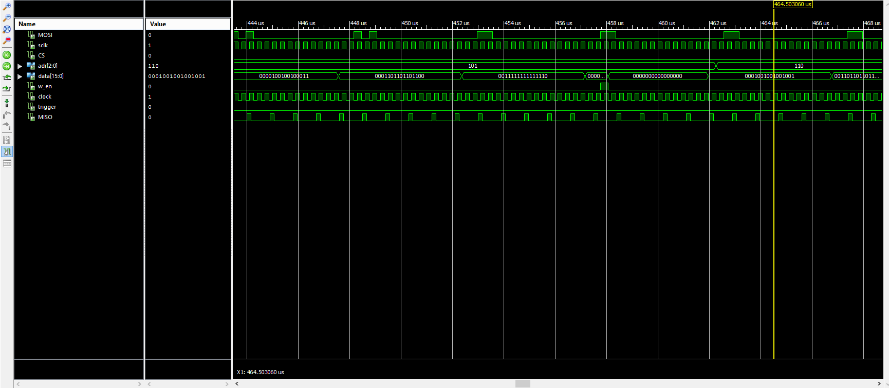
The top-level module is quite simple, it contains the modules needed for each ADC and maps the appropriate I/O for the data to be recorded. One thing to note is we get around the need for a separate bit shifting step by forcing the two MSB to 0 and then discarding the two LSB to get the 14 bits of data we care about.
module ADC_Master(
    input wire clk, // ADC clock in, 8MHz nominal
    input wire trigger, //Update cycle trigger signal
    input wire MISO, // Master In, Slave Out
    output wire MOSI, // Master Out, Slave In
    output wire sclk, //Clock output to ADC
    output wire CS, //ADC Chip select line
    output wire [2:0] adr, //Address to write data to
    output wire [15:0] data, // Data to be written
    output wire w_en // Write enable for data
    );

    wire shift_en, done; // Shift register status comms
    wire add, rst; //Accumulator control lines
    wire complete;
    wire [15:0] acc_in;
    wire [15:0] acc_out;
    wire [2:0] chan;

    assign data = {2'b00, acc_out[15:2]}; //Bitshift 16 bit sum to get 14 bit data
    assign w_en = complete;

    spi_shift shift ( //SPI Shift register module
        .sclk(sclk),
        .MOSI(MOSI),
        .MISO(MISO),
        .CS(CS),
        .clk(clk),
        .done(done),
        .shift_en(shift_en),
        .chan(chan),
        .data(acc_in)
    );

    spi_ctrl ctrl ( //SPI controller
        .shift_en(shift_en),
        .adr(chan),
        .done(done),
        .add(add),
        .rst(rst),
        .complete(complete),
        .write_adr(adr),
        .clk(clk),
        .trigger(trigger)
    );

    ADC_Accum Accum1 ( //Accumulator for oversampling
      .b(acc_in), // input [15 : 0] b
      .clk(add), // input clk
      .sclr(rst), // input sclr
      .q(acc_out) // output [15 : 0] q
    );


endmodule
The module that does the actual interfacing with the ADC is spi_shift. Overall, it’s pretty simple. It shifts in the data written by the ADC on the positive clock edges and creates the address to shift out on the right bits on the negative clock. This allows me to cycle through all 8 channels of each ADC depending on what is requested by the controller.
module spi_shift(
    input wire [2:0] chan, //Channel to shift out
    input wire shift_en, clk,
    input wire MISO,
    output reg [15:0] data,
    output wire sclk,
    output reg MOSI,
    output wire CS,
    output reg done //Done notification line
    );

    reg [3:0] count;

    assign sclk = shift_en & clk; //Only output clock when we need to
    assign CS = ~shift_en; //Invert shift enable to create chip select for ADC

    always @(negedge clk) begin
        if (count == 4'b0010) //Output for next ADC Chan on neg
            MOSI <= chan[2];
        else if (count == 4'b0011)
            MOSI <= chan[1];
        else if (count == 4'b0100)
            MOSI <= chan[0];
        else
            MOSI <= 0;
        if (count == 4'b1111) //If last bit received, signal done
            done <= 1'b1;
        else
            done <= 1'b0;
    end

    always @(posedge clk) begin
        if (shift_en == 1'b1) begin // Shift in data on pos if enabled
            count <= count + 1'b1;
            data <= {data[14:0], MISO};
        end else begin //Otherwise wait
            count <= 4'b0;
            data <= data;
        end
    end

endmodule
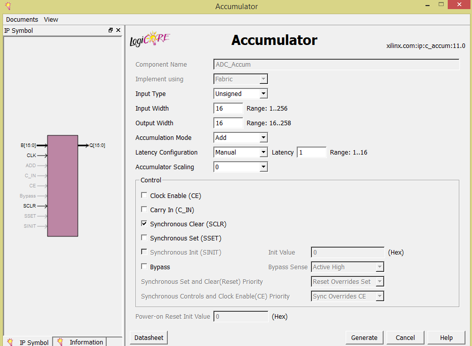
The accumulator is a prebuilt IP that comes free with ISE webpack. Using the graphical IP configurator I set the correct parameters for my use.
The bulk of the action happens in the spi_ctrl module. This is the module that controls the data flow, telling the other modules what to do at the right time. This module is responsible for toggling the data transfer, accumulator reset and the writing of a final value at the correct address. I did this through a state machine with 5 states, with an additional state available if needed. Here’s a code snippet of the “Run” state which is where most of the data movement happens to give you an idea of the code structure.
Run : begin //Main running state
                shift_en <= 1'b1; //Turn on shift register
                complete <= 1'b0;
                flag2 <= flag2;
                if (count == 4'b1111) begin
                    if (flag2 == 1'b1) begin //Use flags to run send only once
                        nstate <= Send;
                        flag2 <= 1'b0;
                    end else begin
                        nstate <= nstate;
                        flag2 <= flag2;
                    end
                    write_adr <= write_adr;
                    adr <= adr;
                end else if (count == 4'b0000) begin
                    write_adr <= curradd;
                    adr <= adr;
                    nstate <= nstate;
                    flag <= 1'b0;
                    flag2 <= 1'b1;
                end else if (count == 4'b1000) begin
                    if (flag == 0) begin //Use flags to increment only once
                        nadd <= curradd + 1'b1;
                        flag <= 1'b1;
                    end else begin
                        nadd <= nadd;
                        flag <= flag;
                    end
                    adr <= adr;
                    write_adr <= write_adr;
                end else if (count == 4'b1110) begin //Update address for shifter
                    adr <= curradd;
                    write_adr <= write_adr;
                    nstate <= nstate;
                end else begin
                    write_adr <= write_adr;
                    adr <= adr;
                    nstate <= nstate;
                    flag <= flag;
                end
            end
All that’s left to be back on track is the digital module HDL. I’ve done most of the planning and it’s much simpler than the analog code. So (fingers crossed) it won’t take me too long to write. Until tomorrow, peace!
Discussions
Become a Hackaday.io Member
Create an account to leave a comment. Already have an account? Log In.