Close
0%
0%

Spread-Spectrum IR Proximity Sensor Module

Interference-resistant sensor for multiple-robot environments

Similar projects worth following
Most people today have between 0 and 1 robots in their homes, so interference between common sensors and other IR devices isn't a huge problem. What happens when you have 10 of them running around? This project aims to create an IR proximity sensor module that has a low-probability of interfering with, or receiving interference from, other devices in its environment using direct-sequence spread spectrum techniques.

The goal of this project is an inexpensive module for interference-free proximity sensing.  IR light is very useful for both sensing and remote control, but can be interference-prone.  I have a remote-controlled lamp, for instance, that will respond to my Roku remote.  More subtle is the degradation of range that can happen when multiple IR devices operate in the same environment, even though they may use different carrier frequencies.  There are no FCC rules governing IR, so every designer is free to use whatever modulation scheme or frequency they wish.  You might not see it, but it's the Wild West between 750 and 1100nm in your house.

Now, we are starting to add robots into this environment, often using sensors in these same IR wavelengths.  When available sensors bother to avoid interference, they sometimes use short pulses of light (e.g. Vishay sensors), but this is not necessarily scalable to many sensors operating continuously.  Additional techniques include polling sensors repeatedly to reject spurious detections.  These techniques are limited in the amount of interference they can eliminate, and multiple sensors operating simultaneously may not be a design goal.

I envision using a direct sequence spread spectrum modulation technique to reduce the probability of generating or receiving interference for IR sensors.  Additionally, these same techniques might be applied to communications.

Basic Idea

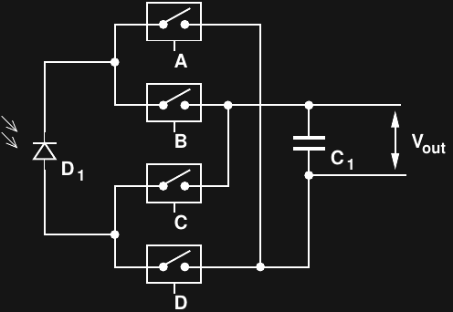
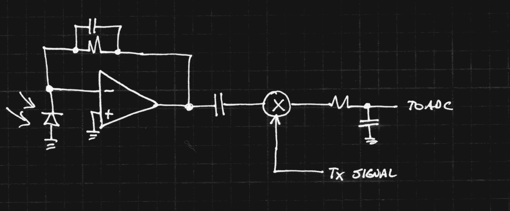
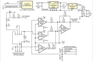
The block diagram shows the basic idea, although several implementations are possible.

Transmit

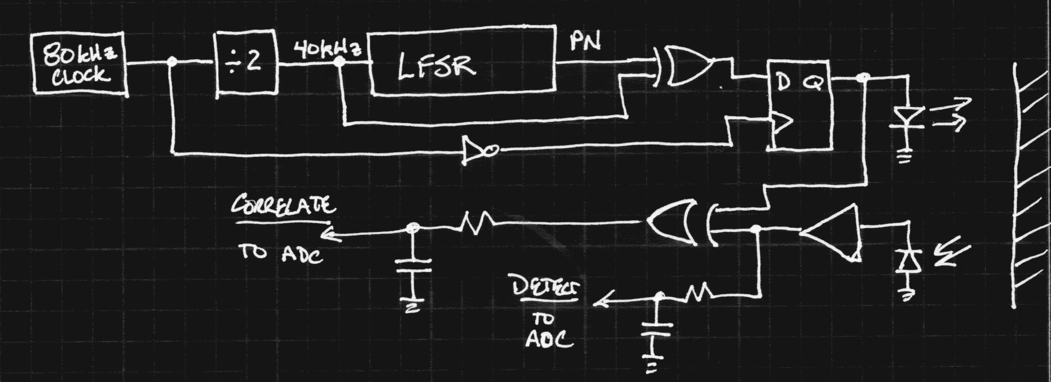
The top of the diagram is the transmit chain.  An 80 kHz clock is divided by two to yield 40 kHz.  The 40 kHz clock is fed into a linear-feedback shift register (LFSR) to generate a pseudo-noise (PN) sequence.  An important property of these sequences is that their autocorrelation function has a single peak - in the simplest of terms, it's difficult to mistake other signals for the one you've generated.  The pseudo-random bit-stream is then multiplied by the original 40 kHz clock in the upper XOR gate, and the result is registered in a D-flop to avoid runt pulses.  The result is a spreading of the 40 kHz signal to cover a wider bandwidth.

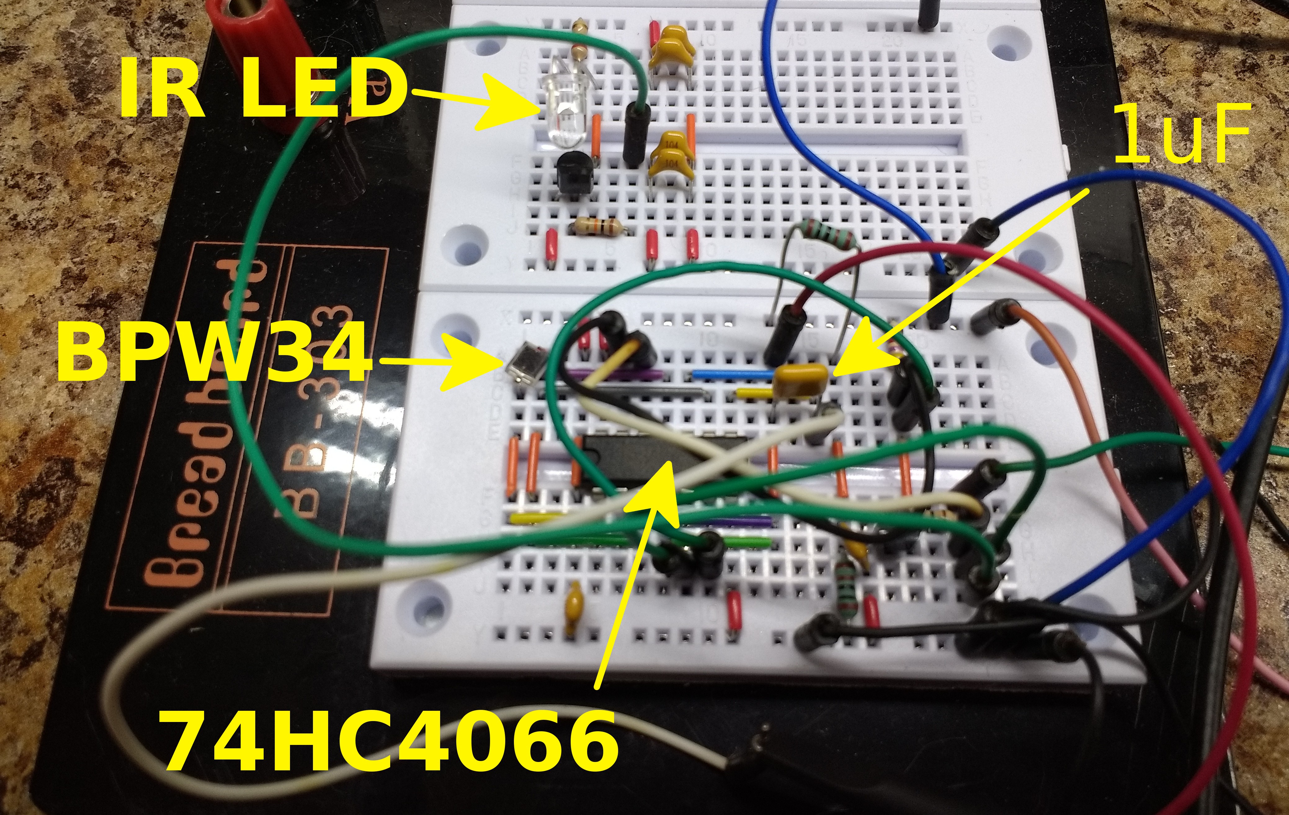
I happened to have a hardware implementation of this modulation scheme already, having built one as the RF exciter for #The Diode Clock.. While it is normally used int the MHz range, it works fine at 40 kHz, too, so I gathered some test data with it.  Here are some waveforms I captured:

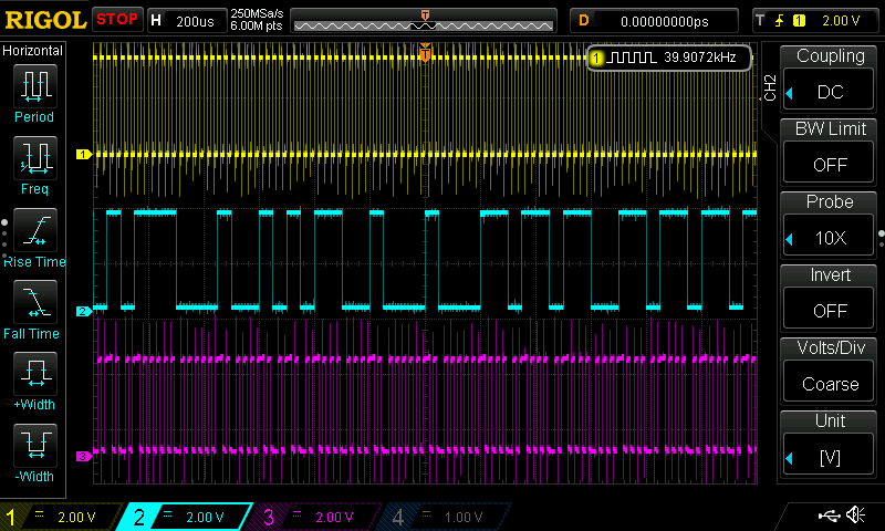
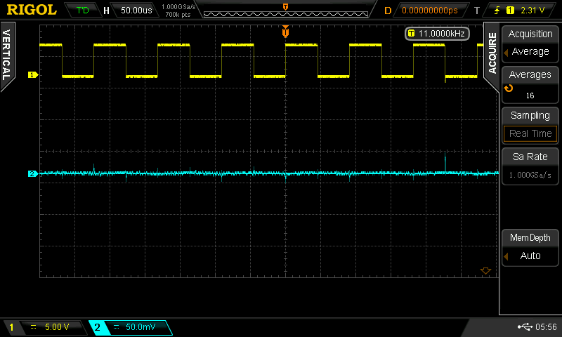
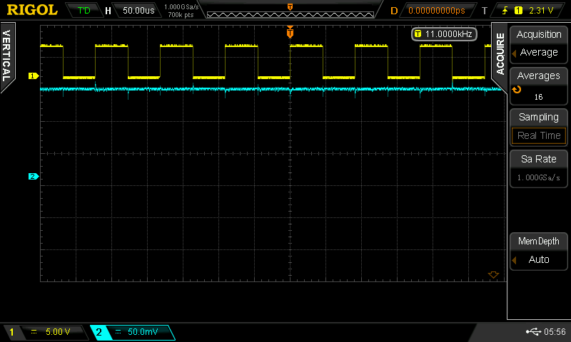
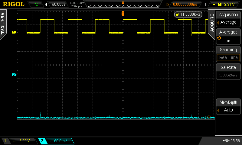
The yellow trace is the un-modulated 40 KHz signal, the cyan the pseudo-random output of the LFSR, and the magenta the modulated output.  A zoom-in shows the output in better detail:

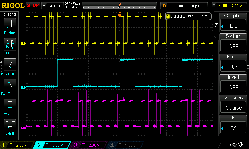
You can see that the PN sequence is selecting the phase of the 40 kHz carrier.  An important property of this sequence is that it can only go so long without a transition, like Manchester encoding. This is important for AC-coupled transmission, so the switching threshold can be tracked accurately.

The hardware I had available uses a 15-stage LFSR, so can generate uniform runs of up to 15 clocks.  Since most consumer IR sensors seem to respond to around 6 cycles of 40 kHz IR, the final LFSR may need to be somewhat shorter.  On the other hand,this document points out that for any LFSR, half the runs are of length 1, one fourth are of length 2, one eighth of length 3, etc.  So only 1/32 of them are of length 6 or greater, which may allow longer sequences.

The result is best visualized with a spectrum analyzer:

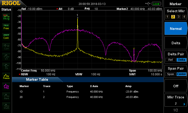
In this case, the yellow trace is the un-modulated 40 kHz signal, while the magenta is the output.  You can see that the energy has been spread across a range of frequencies, with the first zeros at 20 kHz and 60 kHz.  At this resolution bandwidth...

Read more »

  • Lots of tiny PCBs

    Ted Yapo03/27/2018 at 16:33 5 comments

    My breakouts for the various sensors arrived from OSH Park last night, and I got a chance to assemble some of them this morning.  Now, there's a bunch of testing to do.  Those things that looks like buttons are actually IR sensors.  Buttons don't work for detecting IR.

    I also had a deeper look into some datasheets this weekend to see if I could make sense of the level of modulated IR that commercial sensors are capable of detecting, and the implications for this system.

    TSOP38138

    I first considered the TSOP38138 as a reference for comparison.  This is a traditional 3-legged through-hole remote control receiver that claims 45m range, the longest I could find.  The datasheet says that the minimum irradiance (typ)  is 0.12 mW/m^2 (maximum is 0.25 mW/m^2).  It also lists the maximum irradiance (which presumably saturates the photodiode) as 30 W/m^2 (minimum).  That's a respectable 54 dB dynamic range.  This is a narrow-band sensor that receives 38 kHz modulated IR.

    This datasheet also lists correlations between ambient light levels and irradiance on the sensor.  They equate 10W/m^2 on the sensor to 1.4 klx at a color temperature of 2856T and 8.2 klx at T=5900 (daylight).

    TSMP77000T

    Next up is the TSMP77000T, which is one of the parts I'm evaluating for the front-end.  This is a wide-band receiver (20 kHz - 60 kHz) intended for learning remotes.  Since learning remotes are typically trained while close to the original remote, the sensitivity is not very high.  The datasheet claims a 5m transmission distance, which although much less than the 45m of the reference sensor, would still be more than adequate  for my purposes.  The sensitivity is listed as 12 mW/m^2 (typ) and 25 mW/m^2 (max).  This is 1/100 (-20 dB) of the sensitivity of the reference part.  Since light drops off with 1/r^2, you lose half the range for every 6 dB of sensitivity, so you would expect about 1/10 the range (1/ (2^(20/6))), which is close enough to 45/5, so that checks out.

    Overall, his  receiver is probably sensitive enough but the aggressive AGC and limiting digital output isn't ideal for my purposes.

    VBPW34FAS

    This is a surface-mount version of the ever-popular BPW34 diode.  I wanted to see what these irradiance levels would produce for current in a large-area diode like the BPW34.  The datasheet lists the dark current as 2-30nA.  This is the reverse current through the diode you get with no light incident on it.  It further lists the reverse current as 45-55uA at 1mW/cm^2.  This is equivalent to 4.5-5.5 nA at 1 mw/m^2.  At the 0.12 mW/m^2 reference irradiance, this would produce about 0.6 nA of current, which is much less than the diode's dark current.  You can operate the diode in the photovoltaic mode to avoid the dark current issue, but this slows the response dramatically.

    Looking back a few logs at the charge injection estimates for CMOS switches in a direct-mixing receiver, it's clear that you won't be able to obtain good sensitivity with that design.

    ADPD2211

    Finally, I looked at the ADPD2211 from Analog Devices.  This is an interesting photodiode with integrated 24x current amplifier, with a wide bandwidth of 400 kHz.  The datasheet says that 200 nW/cm^2 is required to produce an output with and SNR of 10000:1 (40 dB).  This is 2 mW/m^2, about 0.6x as sensitive as the reference detector, which is pretty good considering the bandwidth, and assuming the reference sensor also achieves 40 dB SNR at the reference irradiance.  The sensitivity certainly seems on par.

    One concern I've had looking at the ADPD2211 is the saturation level, which seems low at 2200uW/cm^2.  This is equivalent to 22W/m^2, which is only a little less than the guaranteed saturation level of the reference sensor.  This is roughly equivalent to 18 klx of daylight illuminant (T=5900K).  Daylight ranges from 10,000-25,000...

    Read more »

  • Charge injection concerns / Shot-noise-limited is good

    Ted Yapo03/24/2018 at 03:03 0 comments

    So I thought about a different CMOS-switch mixing front-end, this one using the photodiode in reverse-bias to speed the response (the previous idea used photovoltaic mode):

    In this version, switches {A, B, C, D} steer the photocurrent into C1 in forward or reverse polarity to mix the incoming optical signal with the local oscillator (or pseudo-noise).  To read out the result, switches {D, E} are closed, allowing the voltage on C1 to be sampled at Vout.  Now that I look at it, the diagram should really be turned on its side.

    After drawing this up, I started to think about the currents involved.  Let's assume the photocurrent is on the order of 10 nA at a low signal level (for lack of a better guess), and that the local oscillator is running at 40 kHz (square wave).  This means that the switches are closed for 12.5us in each polarity.  A current of 10 nA transfers 0.125 pC in 12.5us.  CMOS switches charge injection specs less than this are available, but just barely, and they're not cheap.  You can even find them down in the 0.05 pC range, which seems like it might work OK, but they will drive up the cost considerably.  And that's assuming a 10 nA photocurrent.  Drop that to 1 nA, and all bets are off.

    EDIT 20180324: I missed a decimal place the first time I did these calculations.  It's much worse now!

    Another Commercial Front End

    I happened to stumble across the ADPD2211 photodiode optical sensor.  This sensor offers a bandwidth of 400kHz with shot-noise-limited performance.  Basically, any noise you see on the output is due to the Poisson noise of individual photons hitting the sensor.   That's good.  The IC is a clever 24x current amplifier using current mirrors.  There are two drawbacks I see.  First is the price, $6.61 in single quantities.  That's bad. I think I'll get one just to see what it can do and for a performance benchmark, even if the price keeps it out of the running for the ultimate design.

    The second concern is with the saturation irradiance level.  The datasheet lists the saturation level at 2200 uw/cm^2.  Assuming a wavelength of 555nm, this equates to around 1500 lux, a little more than the brightness of an overcast day (according to Wikipedia).  At first, I thought that this meant the device would have a problem with ambient light levels, but I think this can be fixed by adding an IR filter in front of the photodiode to cut visible light.  This should eliminate most artificial sources of light in indoor environments, since LEDs and CCFLs emit no appreciable IR.  Unfortunately, sunlight has very strong IR components which may still be an issue.

    I think this is close to the ideal front-end for a spread-spectrum IR communications channel, if that tangent to this project should materialize.  There is also the possibility of feeding the output of the ADPD2211 directly to a CMOS switch mixer, since the output is a current.

    The other parts I ordered have arrived, so I can start some experiments, although I'm still waiting on a few breakout PCBs I had to design to work with the smaller parts.

  • Guess what? Front end.

    Ted Yapo03/15/2018 at 23:00 0 comments

    I had a chance to prototype a quick test of the mixer-right-at-the-photodiode idea.  It's a mess both aesthetically and electrically, but it'll do as a PoC.

    The prototype implements this idea for the mixer using a 74HC4066 quad analog switch and 1 uF integrating capacitor (C1):

    It's the same image from the last log, just here for convenience.  On the breadboard, A and C are connected to the input of a signal generator, while B and D are see an inverted copy of the input waveform created by a simple transistor inverter.  A second transistor drives the LED either 0% of the time, 100% of the time, or in or out of phase with the input signal.  I used a BPW34 photodiode and a somewhat random IR LED I had around.

    Here's the output with the LED off:

    The yellow trace is the input from the signal generator, in this case a 11 kHz square wave.  The cyan trace is the voltage across the integrating capacitor.  In this case, the output voltage is very near zero.  This is despite the fact that the shop lights are very bright, and the BPW34 generates 6.4 uA of short-circuit current when tested with an ammeter.

    With the LED on constantly, the output is the same, very close to zero:

    When the LED is driven in-phase with the mixer, the output jumps to around 130 mV:

    and with the LED driven out-of-phase, the output is -150 mV.

    I didn't have a LFSR generator handy for these tests, so this simple prototype would cause all sorts of interference, but it shows that the mixer idea is sound.  It already seems pretty immune to interference from other sources, though.  An IR TV remote right next to the BPW34 just produces a little jumpiness on the output, but no appreciable DC shift.

    I still don't know about the small-signal performance, which I can't really evaluate with the lousy layout of the prototype.  Way too much noise and crosstalk.

    Parts Search

    I'm experimenting with this front-end design, but I still intend to start with Vishay's VSOP98260 amplifier.  I also found that they have receivers with photodiodes and this receiver circuit integrated into a single package.  I'm going to evaluate the TSMP6000TT and TSMP77000TT modules.

    I also found a part made by Broadcom, the HSDL-9100-021, that integrates a matched IR LED and photodiode and includes shielding to reduce crosstalk between them.  This sounds like it might work well with either the CMOS switch mixer idea or the VSOP98260 amplifier.

    Now, I have a few small PCBs to design to get these things mounted on something for testing.

  • More Front End Stuff

    Ted Yapo03/15/2018 at 15:33 0 comments

    I couldn't sleep last night.  At least I came up with an idea (it might be lousy).  I wondered how far forward you could push the mixer (correlator) in this system.  Maybe it could be moved all the way up to the photodiode, analogous to direct-conversion RF receivers?

    In this circuit, two SPDT CMOS switches flip the diode from one polarity across RC to the other, synchronous with the transmitted signal.  Any DC light component will cancel out since the photodiode will alternately charge the capacitor one way, then the other.  In contrast, modulated IR received from the transmitter will be in phase with the switching, and add constructively to charge the capacitor to a DC voltage.  This DC voltage can more easily be amplified using precision op-amps, or even chopper amps, since the detected voltage may be very small in some cases. The operation is similar to direct-conversion RF receivers, where the gain takes place at baseband after down-conversion.

    There could be any number of issues with this circuit, including limitations of the CMOS switches.  Two possible problems come to mind: charge injection and switch leakage currents.  Charge injection is when operation of the switch causes a small of amount of charge to be injected (through the MOSFET gates) into the switch contacts. I will have to look into how well-matched typical switches (on the same device) are in their charge-injection characteristics. If the switches are very well matched, the symmetry of the balanced circuit above should mitigate the effect.  There is also typically a trade-off between switch on-resistance and charge injection, so I may be able to optimize the design by choosing the correct switch.  This Maxim application note discusses these issues and how to select a switch.

    The second problem with CMOS switches is leakage current.  In this case, current leaks through the internal parasitic diodes of the MOSFETs comprising the switch and into the switch nodes.  Again, I can select low-leakage switches and try to find ones with matched leakage currents that will cancel in the balanced circuit.

    After a little thought, I've come up with this alternative, which requires a few more driving lines from the MCU, but should be more versatile:

    In this case, the SPDT switches have been replaced with four SPSTs, controlled with four digital lines {A,B,C,D}.  The capacitor in this case is used to integrate the photo current from the diode.  Four modes are possible.  By closing either {A, B} or {C, D},  the capacitor can be discharged, resetting the integrator.  You do this periodically or at the beginning of a measurement.  With all switches open, the capacitor is disconnected from the diode.  This mode is useful for holding the output constant for readout: it's a built-in sample and hold.  Finally with either pairs {A, C} or {B, D} high, the circuit performs as a mixer in one or the other phase (correlating with a transmitted zero or one).

    Although I probably have to use something a little more exotic for good performance, I have a tube of 74HC4066s around here somewhere that I could breadboard up pretty quick to see if this works at all.  I can use a large-area diode and hit it with a lot of light, too :-)

    References

    http://www.analog.com/media/en/training-seminars/tutorials/MT-088.pdf

    http://www.ti.com/lit/sg/slyb125d/slyb125d.pdf

    https://www.maximintegrated.com/en/app-notes/index.mvp/id/5299

  • Front End Thoughts

    Ted Yapo03/15/2018 at 02:56 2 comments

    My original plan for a front-end was something like this:

    The photodiode is connected to an op-amp in transimpedance amplifier (TIA) mode - this converts an input current into an output voltage.  I've done this before for light meters and such, and it works well, at least at DC.  At higher frequencies, it becomes a bit more complex, although it's well explained in the literature.  The output of the TIA is AC-coupled to a mixer, where it gets multiplied by the locally generated (transmit) signal.  The original thought for this was a pair of CMOS switches, maybe 4066's (or something with lower resistance).

    The upside to this approach is that the amplifier is still linear, unlike the Vishay learning-remote amplifier.  The saturating behavior of that amplifier will degrade the mixing performance and limit the sensitivity of the receiver.

    The mixing approach (synchronous detection) is used in lock-in amplifier designs to ignore background, as described in a technical report by Analog Devices. Their example shows CMOS switches in the mixing role:

    The mixer idea seems sound, but there are several downsides to the transimpedance amplifier as a front-end.  Speed may be an issue, but that can be solved by using a high GBW-product amplifier.  The TIA can also experience gain peaking, which causes ringing on the output, but that can be tamed with a feedback capacitor as shown.  These issues are described in the Hamamatsu photonics handbook.

    The biggest problem with receivers like this is the wide dynamic range of the input signal, which can range over many orders of magnitude.  The DC level (ambient light) in the environment many be much greater than the signal. In Photonics Rules of Thumb, they liken this to watching grass grow on top of the Empire State Building.

    The Hamamatsu handbook has a partial solution: the use of a non-linear feedback element instead of a resistor in the TIA:

    Due to the diode in the feedback path, the circuit yields a logarithmic response over several decades or more.  Of course, the output varies wildly with temperature, so this simple circuit doesn't produce a very accurate log conversion without some kind of temperature compensation.  But for purposes of ignoring the Empire State Building, accurate logarithmic output doesn't matter.  The downside of this conversion is that AC signals are also log-transformed.  A 1 nA AC signal on a 1 mA DC pedestal is going to look vanishingly small on a log scale (log(1e-3) ~ log(1.000001e-3)).

    Another clue comes from a presentation from National Semiconductor, which shows a second amplifier being used as a DC servo to zero out DC bias errors:

    This is a way to remove DC signals from the input, but it still suffers from limited dynamic range, due to the resistor in the feedback path.

    I have wondered for a while if you could combine these two ideas - a logarithmic DC servo.  So, I fired up LTspice XVII and gave it a try tonight.  Here's what I came up with after a little experimentation (these particular op-amps are just placeholders until I figure out what I really need):

    I1 and I2 represent the photo current through the detector,  I2 is a sine wave of 1 nA amplitude, and I1 is the DC component (from lighting in the room).  The DC value varies from 1 nA to 1 mA over the simulation run, 5 orders of magnitude).  U1 is in a transimpedance amplifier role, with U2 servoing out the DC component, except with the inclusion of diode-connected transistor Q1 in the feedback loop.  Transistors like this seem to obey a logarithmic response over a wider range than common diodes.  The simulation looks like this:

    The top plot is the simulated DC photodiode current, while the bottom shows the detected signal output.  The output result is essentially unaffected by the huge range of DC offset. ...

    Read more »

View all 5 project logs

Enjoy this project?

Share

Discussions

Vishnu Mohanan wrote 03/21/2018 at 18:34 point

Interesting! May be I could integrate this into my project when finished :)

  Are you sure? yes | no

Simon Merrett wrote 03/14/2018 at 21:06 point

You couldn't have picked a more attractive string of words for the title. I'm hooked. Where do I sign?

  Are you sure? yes | no

Ted Yapo wrote 03/14/2018 at 21:10 point

Thanks, and also for the like.

We need an automatic project title generator that finds the hottest tech buzzwords and strings them together.  Like Deep Learning Quantum Blockchain.

  Are you sure? yes | no

Simon Merrett wrote 03/14/2018 at 21:14 point

But you've come up with a better algorithm because it down-weights terms associated with click-bait. Bottle it and sell it, quick!

Seriously, though I'm interested in the data transmission potential here. Could I follow along in a less vicarious way and perhaps try to reproduce some things in order to show mortals can get in on this? Don't want to be a handbrake but also keen to maximise related benefits of this development.

  Are you sure? yes | no

Ted Yapo wrote 03/14/2018 at 21:26 point

Yes, there are communication applications also, but they are a little more complicated because you have to recover the synchronization.  The same property that makes it interference-resistant also forces you to synchronize the TX and RX LFSR's exactly.

There is plenty of literature on the subject, and even some open implementations in the amateur radio community, but it ain't simple.  I kind of mentioned communications applications in the margin for that reason.

  Are you sure? yes | no

Ted Yapo wrote 03/14/2018 at 21:28 point

Oh, yes, follow and experiment.  It's all open.  All good.

  Are you sure? yes | no

Similar Projects

Does this project spark your interest?

Become a member to follow this project and never miss any updates