 Andrew Ferguson
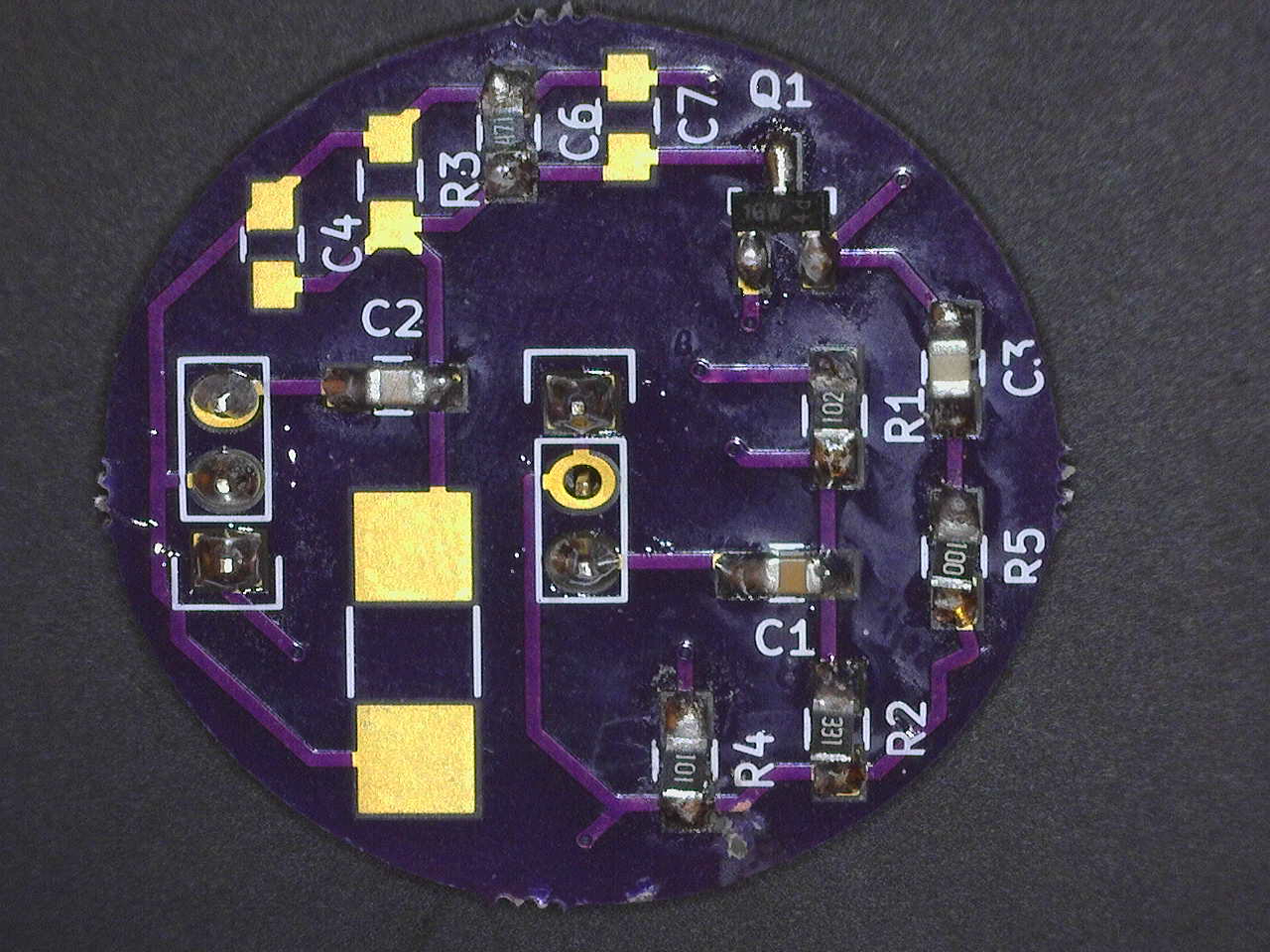
After breadboarding the amplifier for the ultrasound signal and seeing that it worked fine I decided to get some PCBs made from OSH Park. Here's a picture of the soldered up PCB which still consists of a single transistor common emitter amplifier. The reason it is a 1 inch diameter circle is that it will be directly soldered onto the ultrasound transducer and look prettier that way. There are some unsoldered parts here because I want to play with making it a tuned amplifier, by having a parallel resonant circuit as the collector load, but I didn't test this yet. The input pins are in the middle and the output and power pins to the left. The transistor is a BC847 in a SOT23 package, chosen since it is a general purpose npn bipolar. The resistors and capacitors are in 0805 packages.
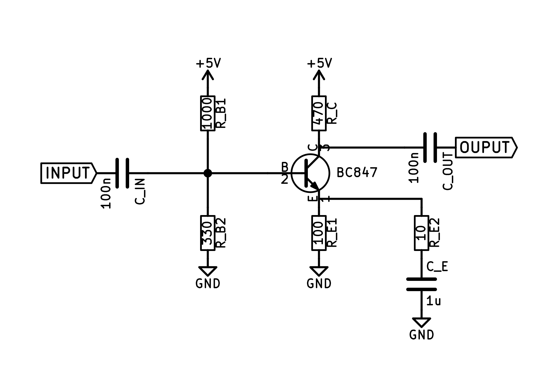
The circuit diagram is as follows, I changed the degenerated emitter to include a resistor (R_E2) in series with the bypass capacitor (C_E) as I hoped this would give me more predictable gain.
The measured gain is as follows, for an input amplitude of 10 mV. Gain compression starts to occur at an input amplitude of 50 mV, much more than I am expecting from the ultrasound receiver. I'm still pretty happy with this design which is now giving a voltage gain of 28 at 200 kHz (the transducer frequency) and next will play with tuning the collector load to reduce out-of-band noise.
Discussions
Become a Hackaday.io Member
Create an account to leave a comment. Already have an account? Log In.