 Robert Hart
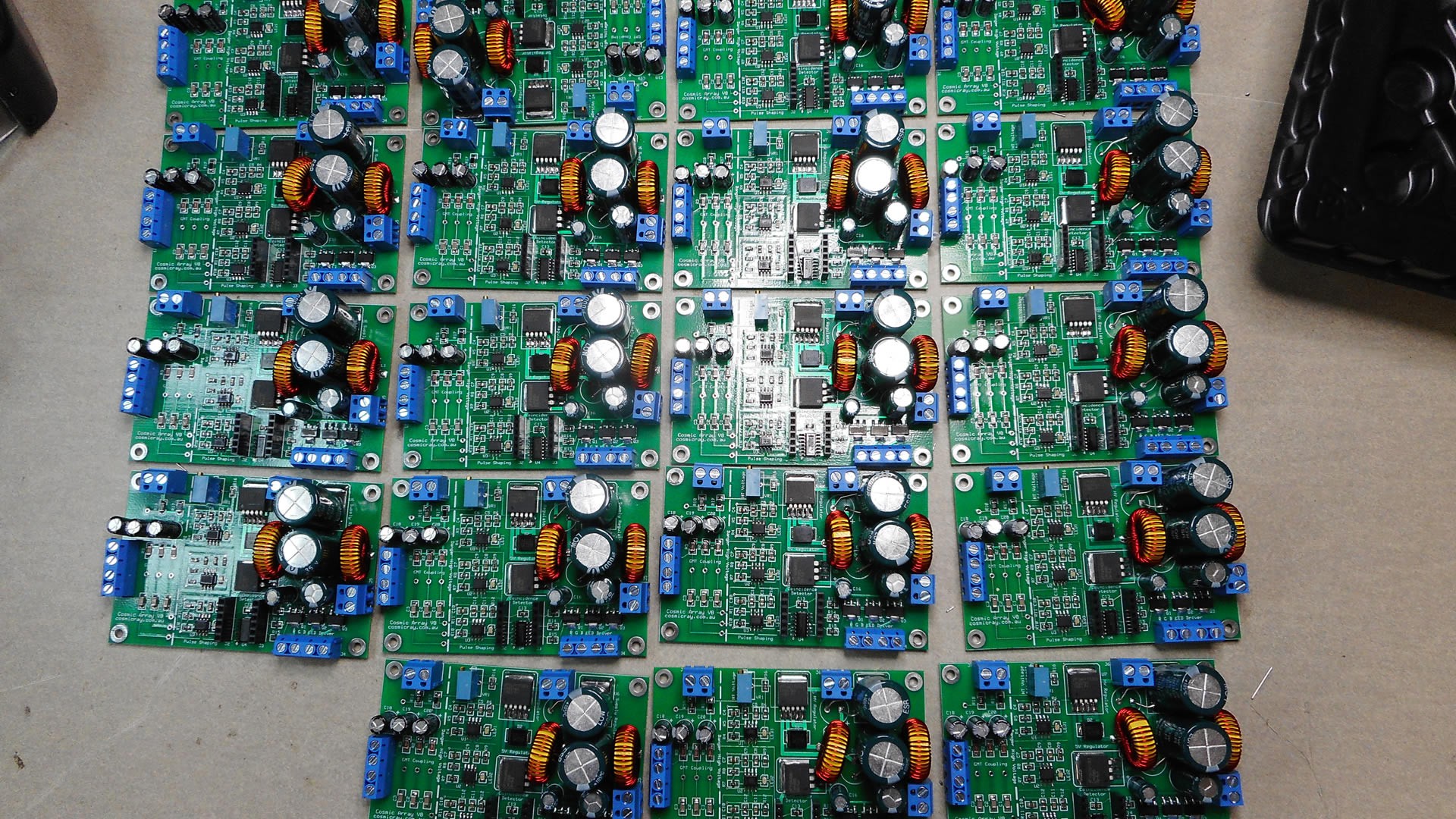
After building many, breadboard, ratnest and prototype designs to test out a number of different approaches. It's become very clear that I need to knuckle-down and start developing a number of PCB prototypes on a multilayer pcb using all SMD components.
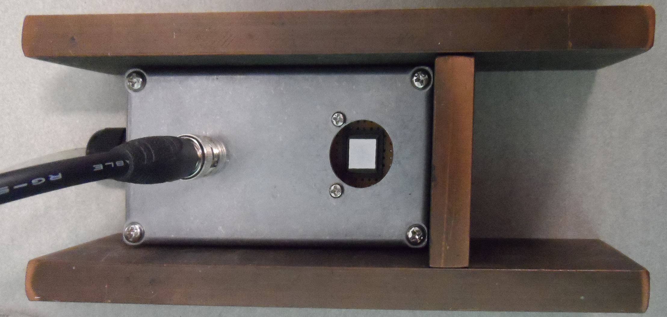
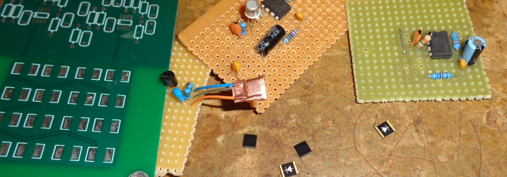 As both the input impedance and gain required on each Si Pin Photodiodes is extremely high and so not only is noise an issue including feedback, crosstalk and vulnerable to RFI, it is also affected by static electric fields. This will becoming an even greater problem when arranged in a multi element array.
 From my last project experience I found that although the PCB CAD package I was using was fast, very easy to use and free, I couldn't import component footprints CAD files nor export Gerber pcb files. Meaning I had to a number of custom footprints and could get competitive pricing when needing to have multiple PCBs manufactured. As will be the case again for this project I'm making a move over to KiCad EDA. The disadvantages are learning a new CAD package but so far so good.
Discussions
Become a Hackaday.io Member
Create an account to leave a comment. Already have an account? Log In.