PCB Layout...
There was some back and forth about how many layers the PCB had to be. For keeping things cheap, the obvious choice would have been to use a 2 layer board. However, there needs to be a balance between being cheap and being simple. Sometimes to be simple you have to be a bit "anti-simple". The decision was then made to use a 4 layer board as it has significant benefits:
- Meets size constraint for part placement and routing
- Ample room for thermal management without traces in the way
- Routing got VERY easy
- Gives way for large planes
- Very important in the overall design
- Does not require the need for bus bars or external power distribution. The boards themselves can carry the required current.

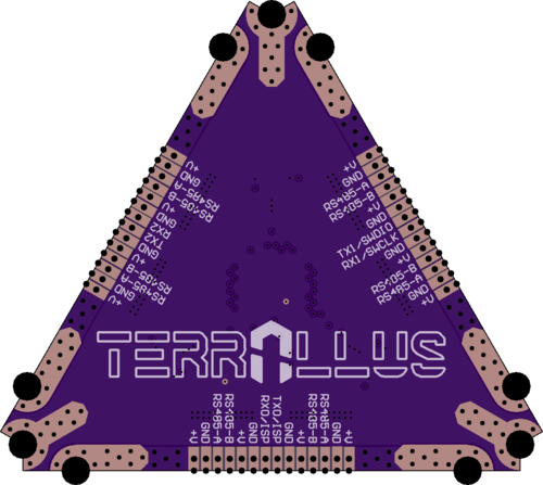
The PCB stack up is as follows:
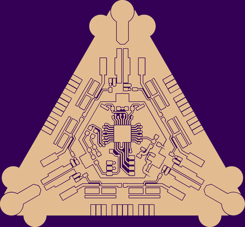 | Top Layer - Contains all the electronic components - Poured as "+V" to provide a large current path for adjacent cells |
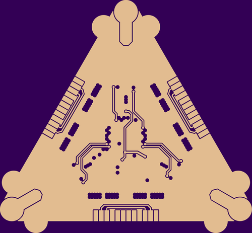 | Signal Layer 2 - Contains 3.3V distribution and PWM control traces. - Poured as "+V" to complement the Top Layer plane. |
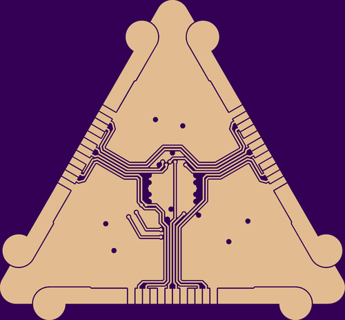 | Signal Layer 3 - Contains all RS485 and UART lines interconnecting the 3x edge connectors. - Poured as "GND" to provide a large current return path as well as thermal distribution plane for the LEDs. |
 | Bottom Layer - Poured as "GND" to complement the ground plane in the previous layer as well as a uniform thermal plane for heat sinking. |
PCB Features...
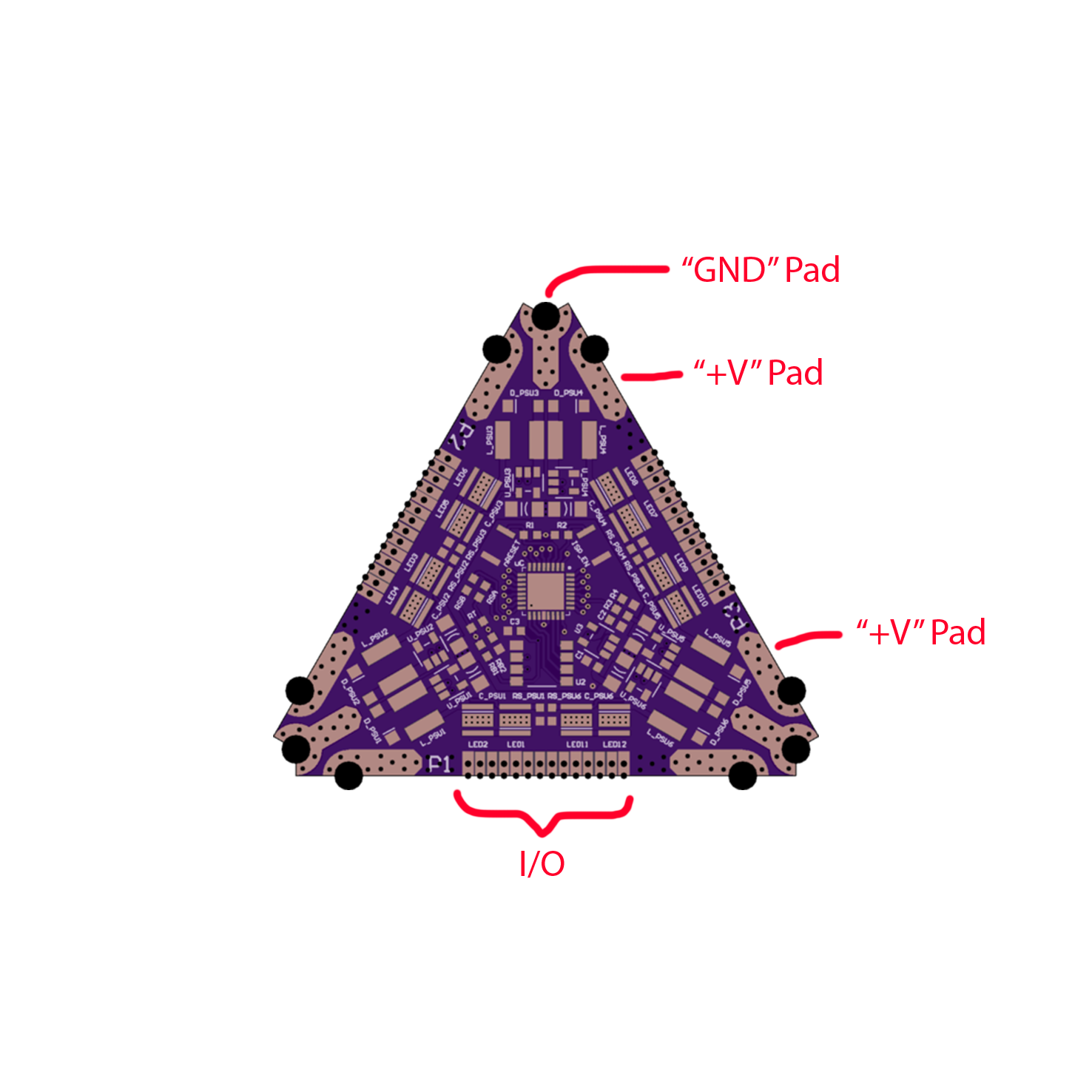
The PCB has pads attached to the "+V" and "GND" plated M3 screw holes to allow up to 12 AWG wire to be directly soldered. With the help of the large power planes in the board, there is no need to have external power distribution between cells. The pads are identical on the bottom layer and enable various mounting options such as carrier boards, spring contacts, direct wire to board soldering, etc.
The I/O connector is symmetrical in design. It can be used in any orientation with other cells and facilitates the use of wires, flat cables, headers, spring contacts or direct "butt" joints with adjacent cells. Power can either be applied with the screw hole pads or the I/O connector. When assembled as an array, it is recommended to use the screw hole pads for the initial power entry into the array and the I/O connectors within the array.
 slisgrinder
Discussions
Become a Hackaday.io Member
Create an account to leave a comment. Already have an account? Log In.