 Spencer
When V1 failed it was nearly a year before tried again. I redid all the logic design portion as well making liberal use of logic Friday. The file is include in the Git hub. I then recreated the diagram in dip trace. However this time I had a new trick up my sleeve. I figured out how to use hierarchy blocks and was very generous in their usage. This made the schematic a lot cleaner witch for a project this large helps keep mistakes at a minimum.
This time I learned from my mistakes. I printed out the schematic and went though the first few numbers to make sure the out put was as expected.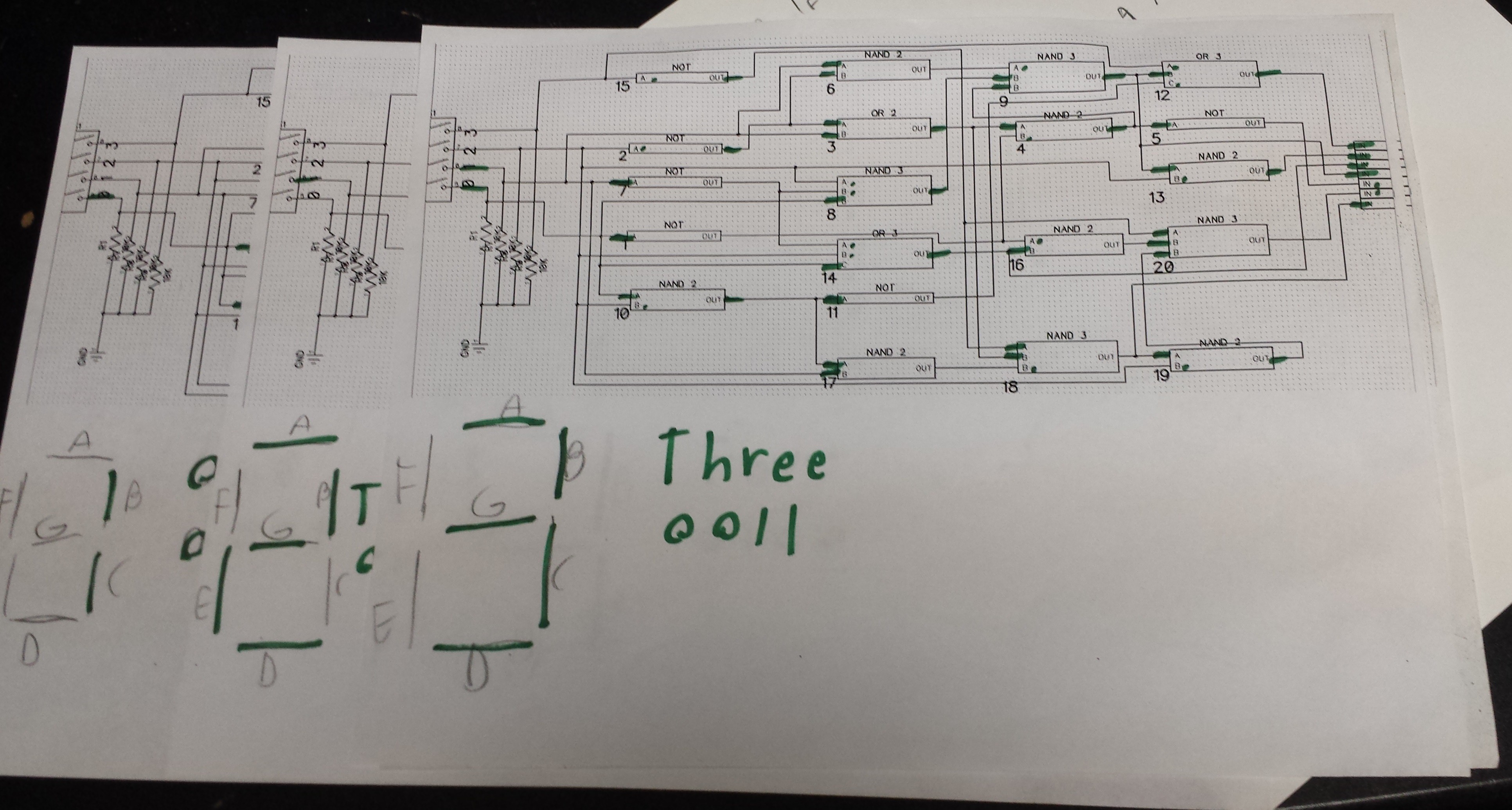
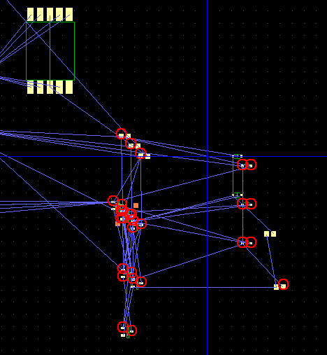
With the knowledge the the core was sound I moved onto the actually PCB portion. I was hoping all the parts would be grouped close to their respective gates but I was massively disappointed. Turns out all the parts were directly on top of each other. As you can see in the picture below there are stacks of fets 2-5 fets deep.
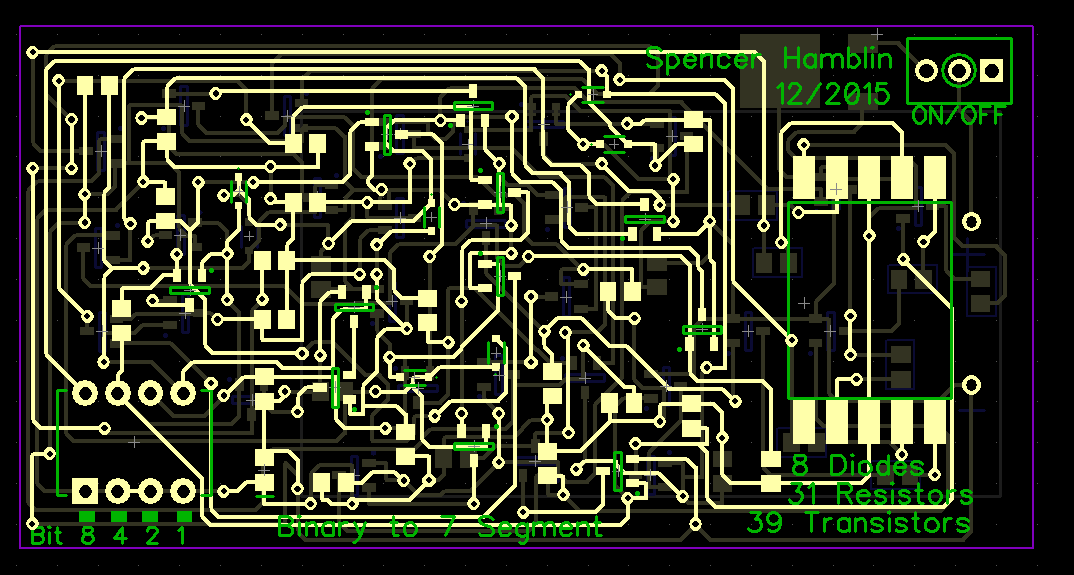
I still took a shot at manually routing it but after getting frustrated I give in to the auto route. Initial results were pretty bad. I played around with it quite a bit but I managed to get it working reasonably well. The resulting PCB was ~5 square inches. I think it would be possible to get is smaller but that is getting close to the limit. The auto router did have to chew on it for a few minutes.
The final result
Discussions
Become a Hackaday.io Member
Create an account to leave a comment. Already have an account? Log In.