 Arduino Enigma
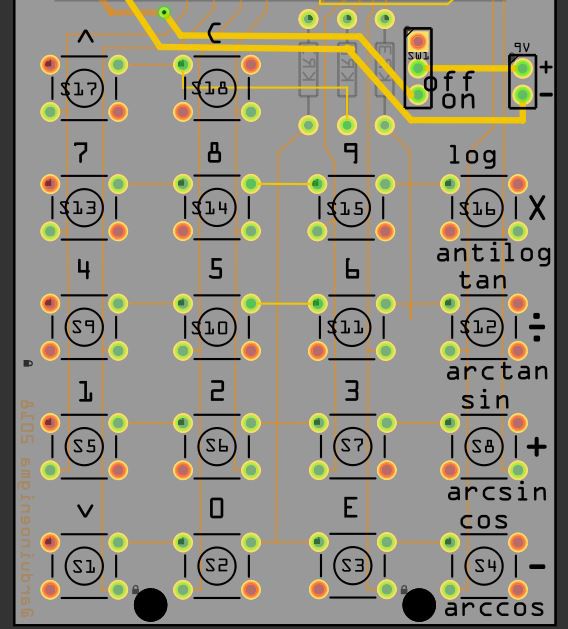
It is becoming evident that V1 is a little too wide. The PCB is cut to the width of the resistors, the power plug is moved inwards and the scientific function labels are moved above and below the keys. For this board, a keyboard mask is created. The board will be ordered with white soldermask and black silkscreen to resemble the calculator.
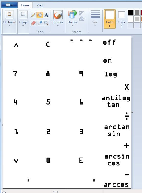
Here is a picture of the layout. What follows below are the instructions on how to create a negative mask using Fritzing, the Sniping Tool and Paint.

First, design the layout of the labels to appear. Don't worry too much about final location, labels can be moved and deleted later. Just make sure all the labels you want are drawn at this point.
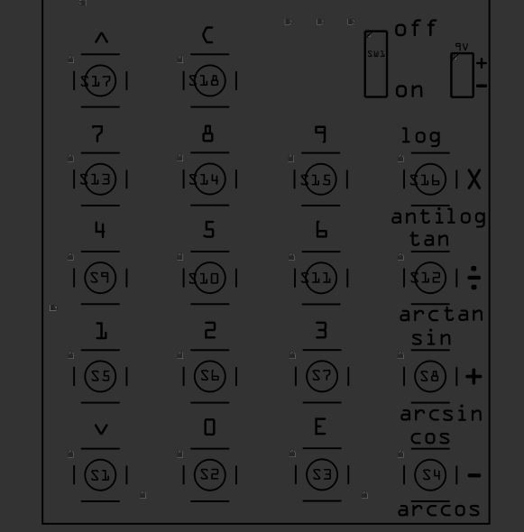
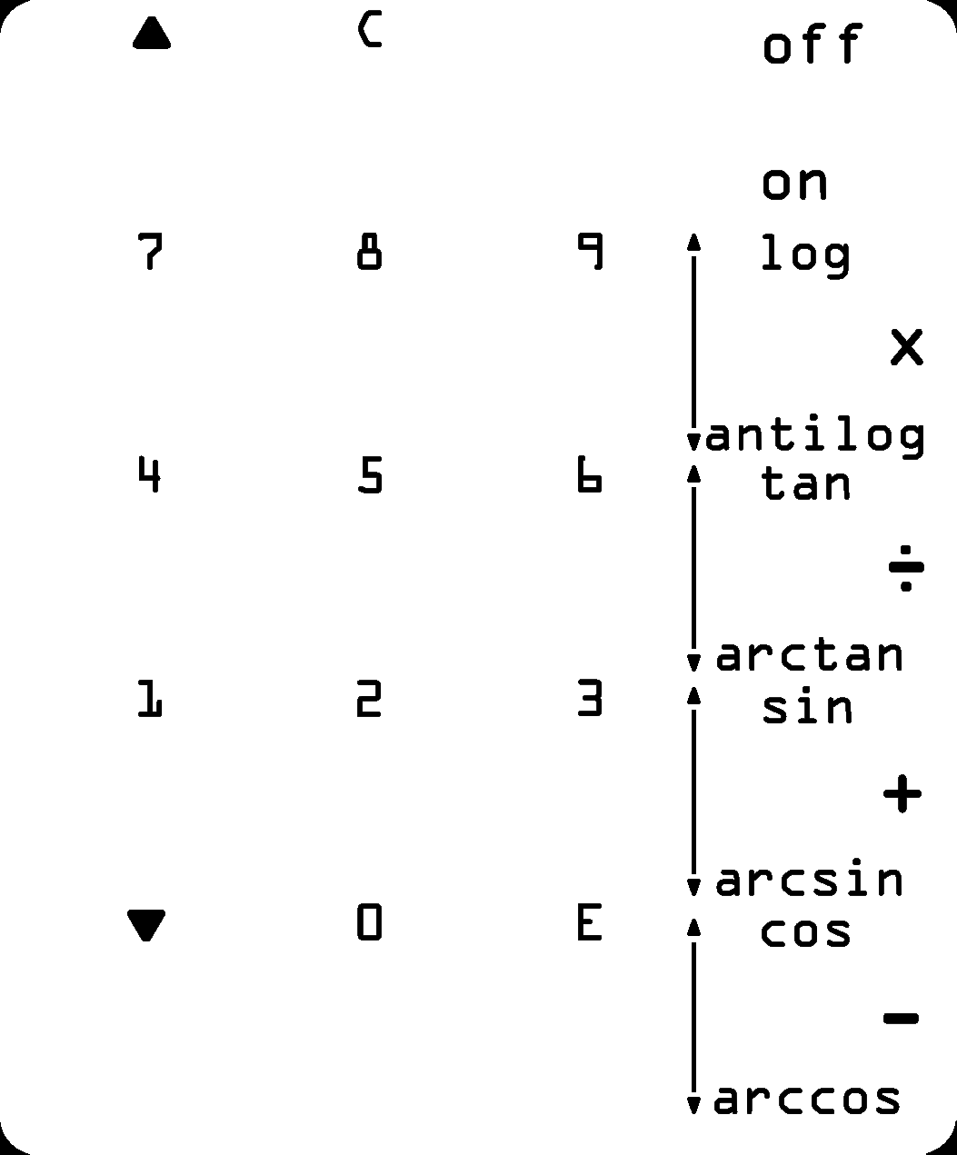
Then, turn all the layers off View->Hide All Layers and then turn on only the top silkscreen View->Silkscreen Top Layer
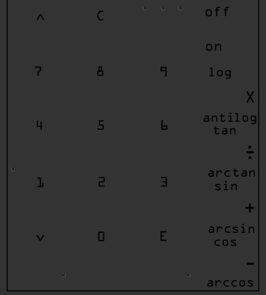
To help the cleaning process later, the buttons can be deleted at this stage. Just make sure to save the file first and then revert to the saved file. The goal of this step is to minimize the amount of editing in Paint. A few stray marks are ok, they can be deleted later.
Then, using the Sniping Tool, capture the keyboard area.
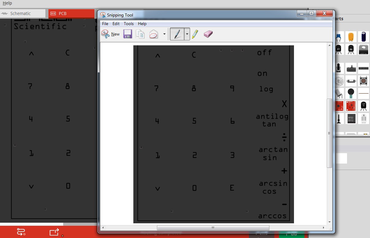
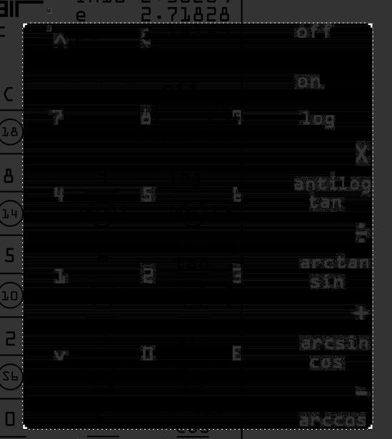
Without saving anything, go to Paint and select Paste (Ctrl+V)

Click on Color 1 and click on White. Then click the Bucket Tool and click on an empty area of the picture to paint it white.
Zoom in and paint inside any closed letters. Any undesired marks can be deleted at this step as well with the Eraser tool.

Rounded corners and any desired artwork can be added at this step. The location of the text labels can be fine tuned also. If you want to add a logo like the OSHW gear, do it now.
When ready, save as PNG, if the file is saved by mistake as a JPG, compression artifacts will be visible when imported into Fritzing. If this happens, go back, press (Ctrl+Z) to undo a couple of steps, save as PNG and redo the last couple of fixes that were undone.
If the file is saved as PNG, a lossless format, it will look nice and clean when imported into Fritzing.

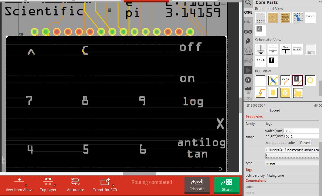
To import the keyboard mask into Fritzing, go th the Core Parts bin and drag a Silkscreen Image into the PCB view.
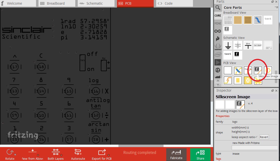
Then load the file we have been working on. To do that, go to the Inspector window and click the button above "image"
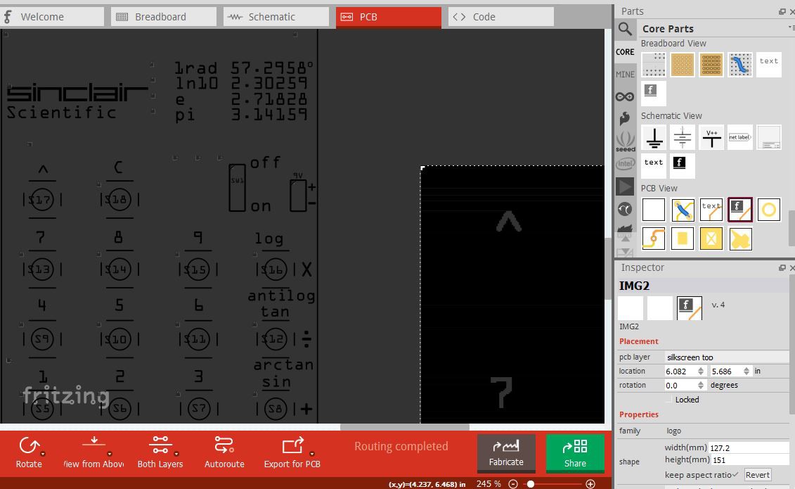
The image has been imported at its native DPI, to make it wit, set approximate width and x-y location. A good initial width is one a little less than the PCB, 49mm.
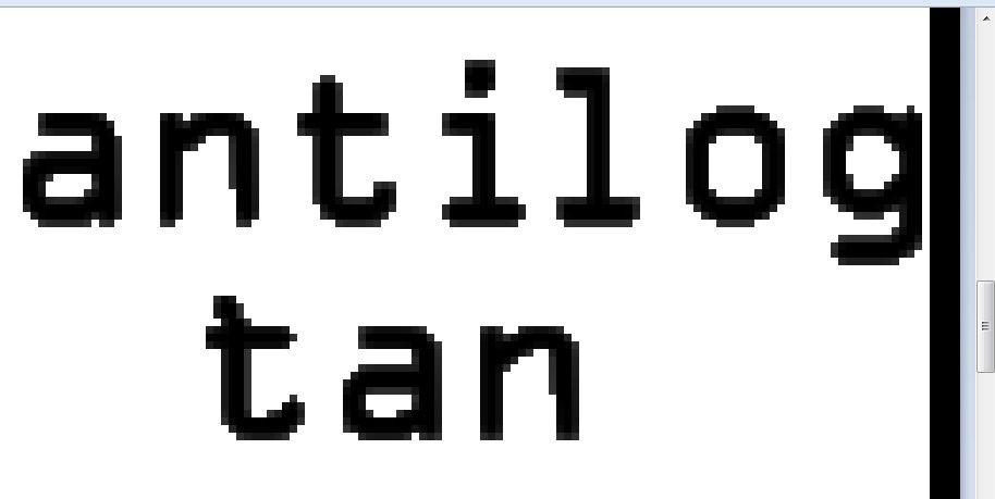
Then align the character on the top left corner so the hole in the image and the silkscreen image overlap. Notice that towards the right, the labels do not align. Its time to fix that by finding the exact image width to use.

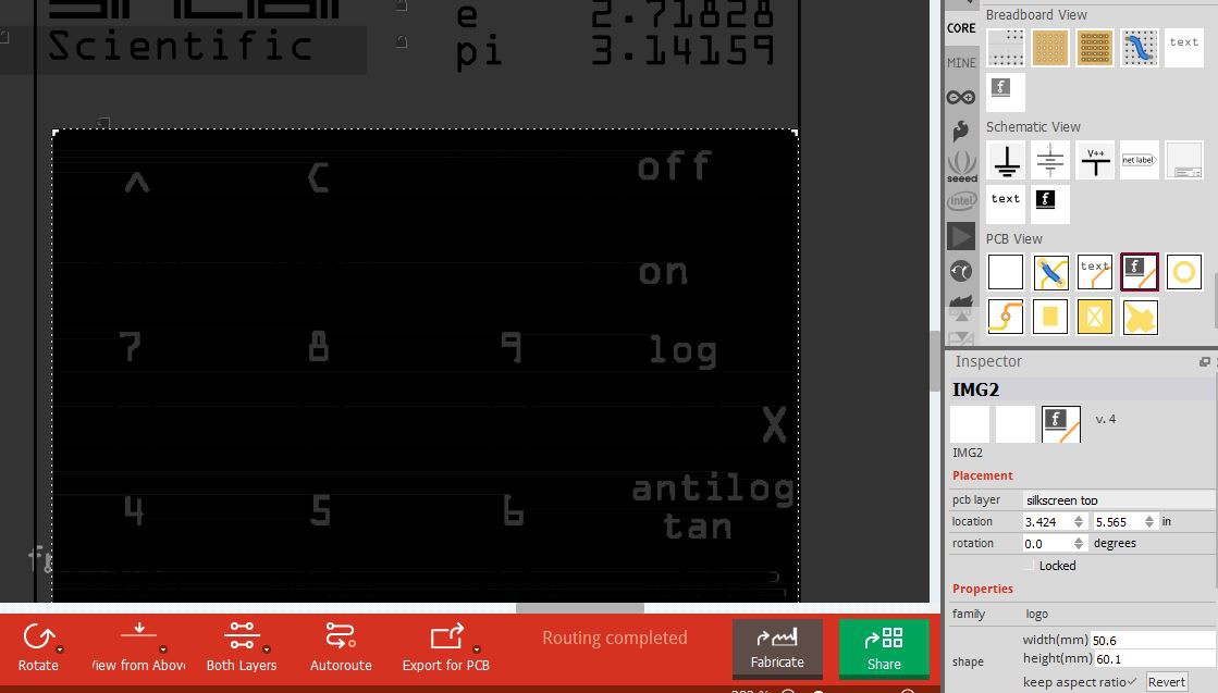
Trial and error yields 50.6 as the value that makes all the labels align. The image can be repositioned to make sure the top left label still fits well.
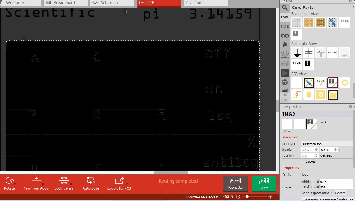
Note the x and y location values and move the image out of the way. Now its time to delete the silkscreen labels that were above the components.

Finally, move the image back to the previous location. There are no visual clues as to what is the desired location, that's why we noted them on the previous step.
Finally, to verify that the alignment is correct, turn all the layers back on. Select the Bottom Layer as clickable and select View from Above. Any issues with the size of the image can be resolved by editing the file in Paint.
To make the image appear narrower without affecting its true width or calculated location, go to Paint and add a black line on the right and save it (as PNG)
Import the image again. The value for the width will be reset to the image size. Set it to the previously determined value of 50.6 and see the result. At this point, I would go back to Paint, move the antilog label to the left and add more black lines on the right.
Repeat until satisfied and then click Export for PCB -> Extended Gerbers.
As previously shown in this project log, it does not hurt to tent the vias.
The procedure is copied below for your convenience.
Fritzing Tips:  Tented Vias

-Save Work

-File->Export->For Production->Extended Gerber, create "tented" folder

-Routing->Select All Vias

-Press Delete key

-Export Gerbers to no-vias folder

-File->Revert

-Copy maskTop and maskBottom files from no-vias to tented folder
At this stage, I like to submit the file to Oshpark.com to create a rendered image of the our hard work. If any issues are identified here, go back to Fritzing and correct them. Once satisfied, make the board!
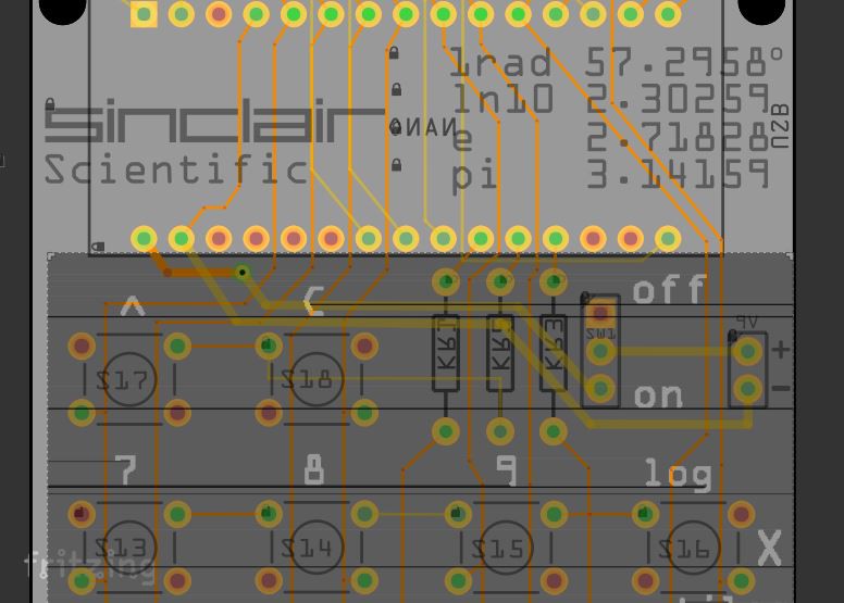
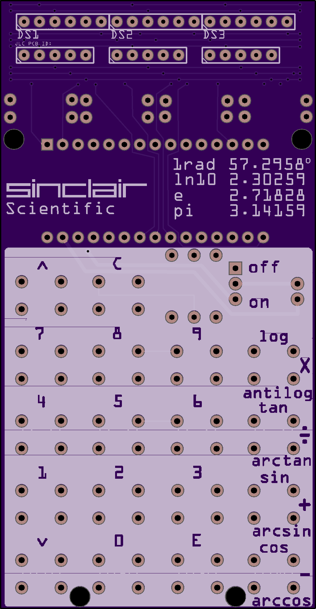
This is an image of the actual V2 board that was ordered, Notice how the tracks going through the front were arranged into a Voltron pattern to go in between the logo and the constants. The goal for future boards is to have no visible tracks running through the keyboard or the Sinclair logo area. Rounded PCB corners would be nice as well, but that is a matter for a different project log.


Discussions
Become a Hackaday.io Member
Create an account to leave a comment. Already have an account? Log In.