 Arduino Enigma
The Gerber files for this version can be downloaded here:
https://oshpark.com/shared_projects/HpVh3N0L
The remaining connections from the Arduino Nano to the current limiting resistors, the LED display common anodes, and the keyboard lines have been routed.
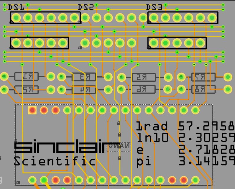
Since there are vias everywhere, connecting a via to an arduino pin is not particularly difficult if both layers are used and one is not picky about which particular pin to use. Lighting up the correct digits will be done in software later. What I did not know at the time is that the A7 and A6 pins are input only. The A7 pin ended up being used to select digit 1 on the left most display. You can see the wire running through the S in the Sinclair LOGO to a via under DS1. Pin A6 was used to select digit 2 on DS1, it runs through the f in the word Scientific. All of the Arduino Nano I/O pins were used except for D0/RX and D1/TX
The vias at the end of the horizontal bus bars on the display are at this point there just for aesthetic purposes. On the keyboard part of the layout, deleting them allowed for the design to be optimized and mostly run on the back side of the board.
8 I/O pins: Connected to one side of the current limiting resistors (output). Connected to the return lines on the keyboard (input).
9 pins: used to drive the common anode of the LED displays (output). Displays the selected character formed by the 8 I/O lines in the desired position.
3 pins: Keyboard row selection (output). Used to select a row of switches, if a switch is pressed, it will be read as low on one of the 8 I/O pins used to drive the display. The internal pull up resistor on the Nano is enabled during this operation to allow the key presses to be read as low.
This design uses 20 pins. The nano has 22 I/O pins (of those A6/A7 are input only).
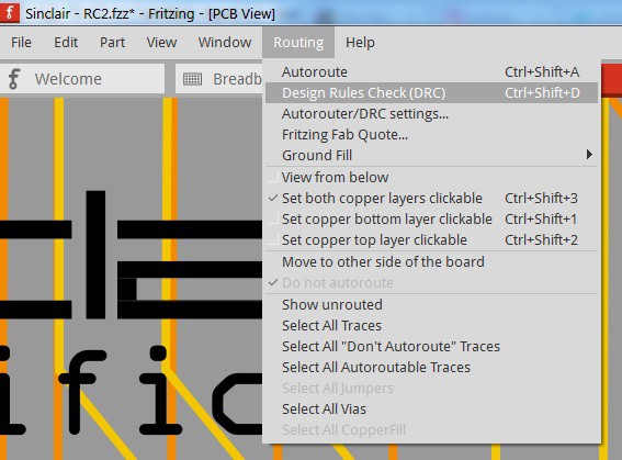
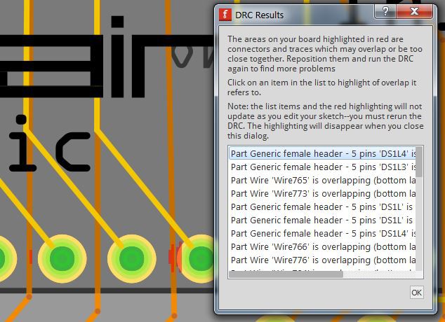
Before submitting anything, run the DRC (Design Rules Check) to ensure all traces are sufficiently separated.
Here are three traces passing in between pins. The one in the center is sufficiently separated from both pins. The one on the left shows a little red where it gets a little close to a pin. Sometimes, even with the align to grid feature turned off so that things can be moved very precisely, it is impossible to get the trace completely away from the pin, the red mark will move from the right side to the left side when the trace is moved a minute distance. In that case, its ok to leave as is. The track on the right is way too close to the pin, there is red everywhere. That one needs to be fixed.
Finally, it time to export the gerbers and upload to Oshpark.
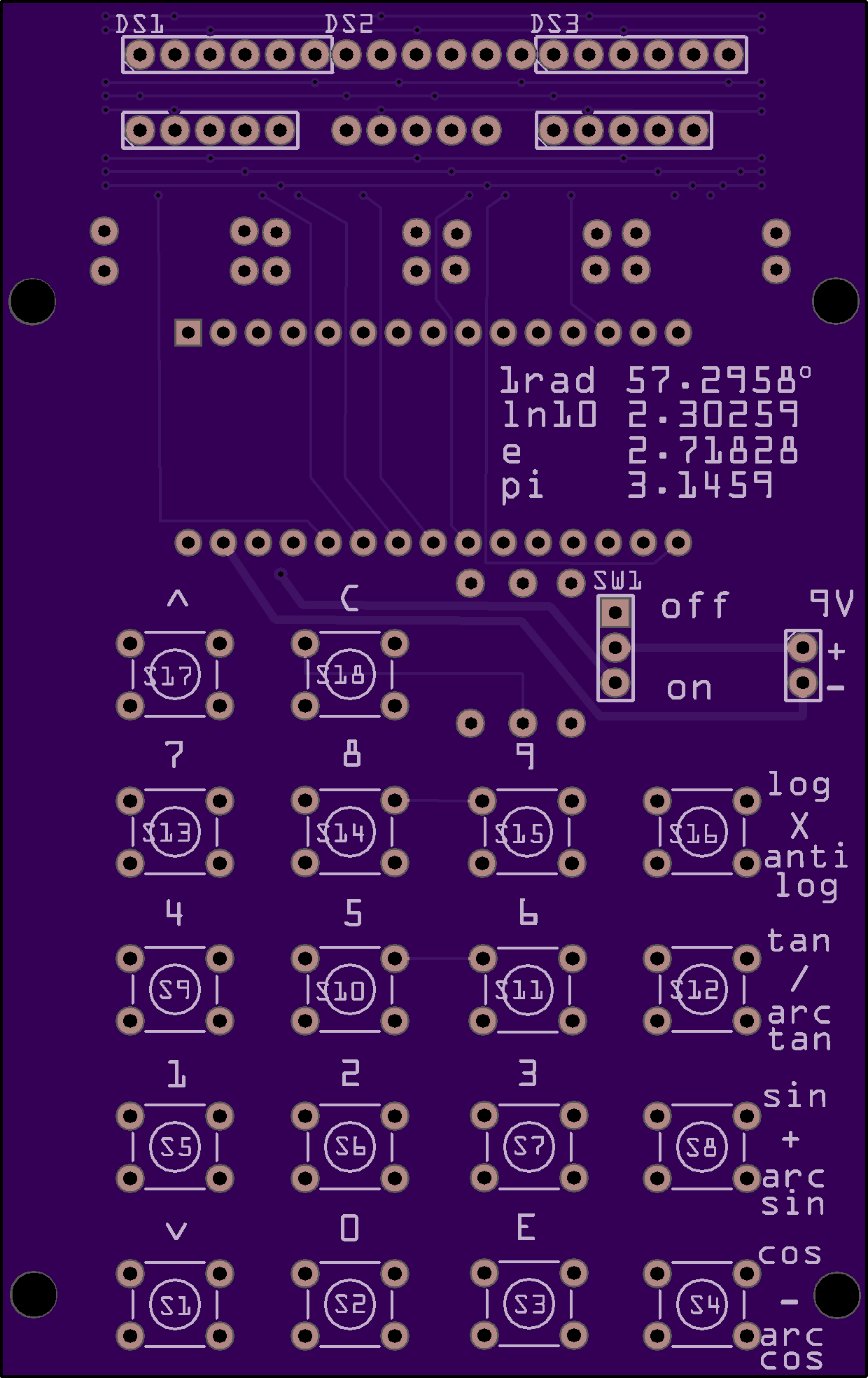
Here is a rendering of the PCB Front:
Oshpark rendering of the PCB Back:

These are production boards, so a couple of extra steps are needed to place soldermask over the vias (tented vias). Two Gerber exports are going to be made, one with a full board, the other for the same board with the vias deleted. Each export goes into a different folder. Luckily, Fritzing supports an easy way to select all the vias. Save your work prior to deleting the vias and then revert to the saved file after the Gerber export is completed.
Once the two set of Gerber files are created, the soldermask files, and if desired, the sikscreen files from the no-vias folder can be copied to the vias folder. I have used this technique with multiple fab houses and it always works.
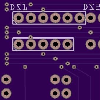
A default Gerber export will have exposed vias:
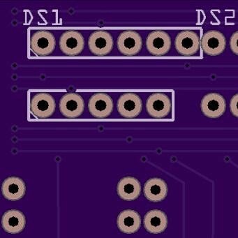
This is what Tented Vias look like. I did not copy the silkscreen file from the no-vias folder, so a discountinuity can be seen on the lower connector for DS1. By also copying the silkscreen file, a continuous line can be drawn over a via.
Fritzing Tips: Tented Vias
-Save Work
-File->Export->For Production->Extended Gerber, create "tented" folder
-Routing->Select All Vias
-Press Delete key
-Export Gerbers to no-vias folder
-File->Revert
-Copy maskTop and maskBottom files from no-vias to tented folder
Time for a quick instagram post:
Discussions
Become a Hackaday.io Member
Create an account to leave a comment. Already have an account? Log In.