 Arduino Enigma
This guide will show the steps to create a custom PCB shape that can be used in Fritzing. In this case, the shape will be a rectangle with 3mm radius corners. This is enough to not have sharp corners, but not so big that it takes away from the usable PCB area.
First, launch Inkscape:
if you don't have it, download it at: https://inkscape.org/en/release/
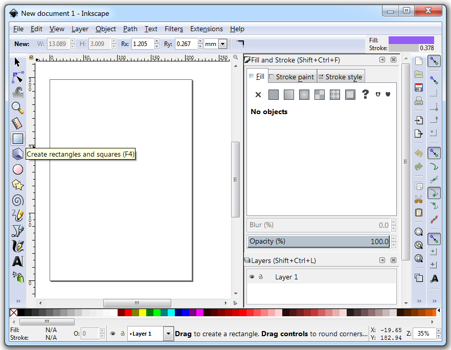
Then click on the Rectangle Tool on the left and draw a rectangle by dragging the mouse. At this point the size is not important. The precise dimensions will be entered in the next step.
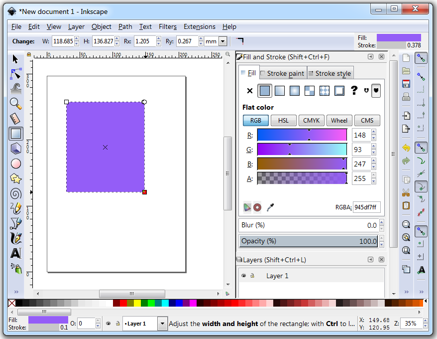
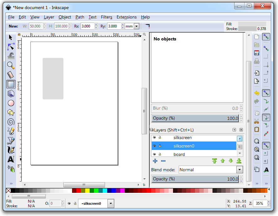
While the rectangle is still selected, enter its dimensions in the boxes above the drawing area. We will make it a 50x100mm rectangle with 3mm radius corners.
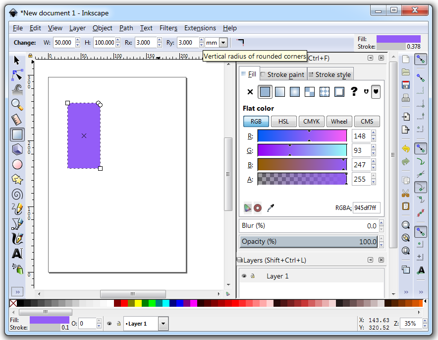
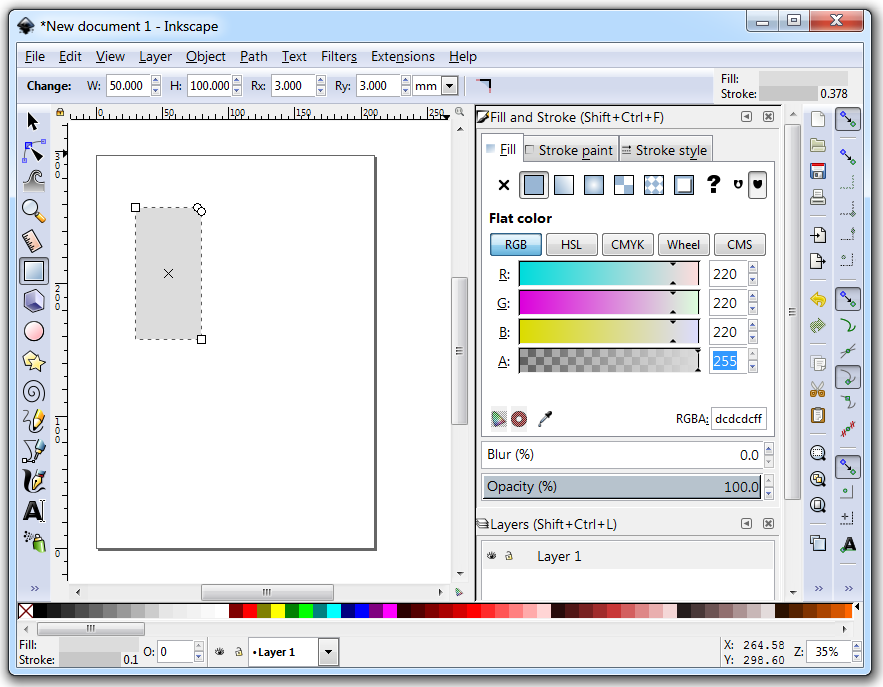
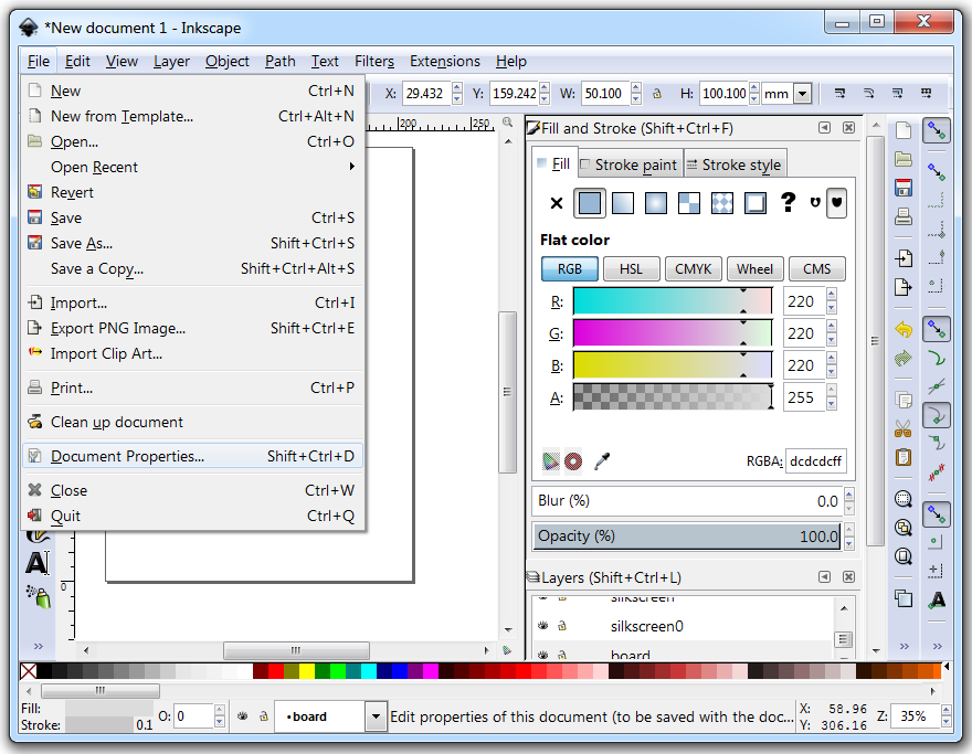
You will be staring at this rectangle for hours. So you can keep the rectangle this nice purple or select a color that's easy on the eyes. To do that, go to the Fill and Stroke window and use the sliders to select the desired color. I made them the same value to get a light grey. Leave the Alpha value (opacity) as 255.
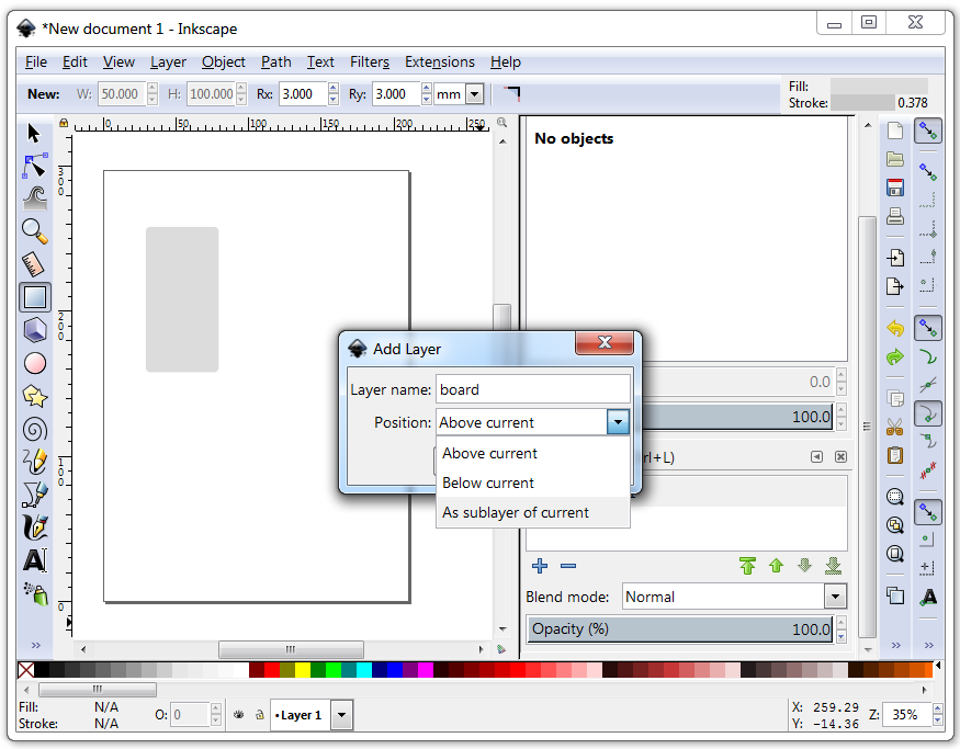
Now its time to add three layers under the current layer. Start by adding one as a sublayer of the current one, name it "board". These are only the visible names. Fritzing needs the layer ID to be named board, silkscreen and silkscreen0. I have not found a way to edit that in Inkscape, so this will be fixed later using Wordpad (or Notepad++ if you prefer).
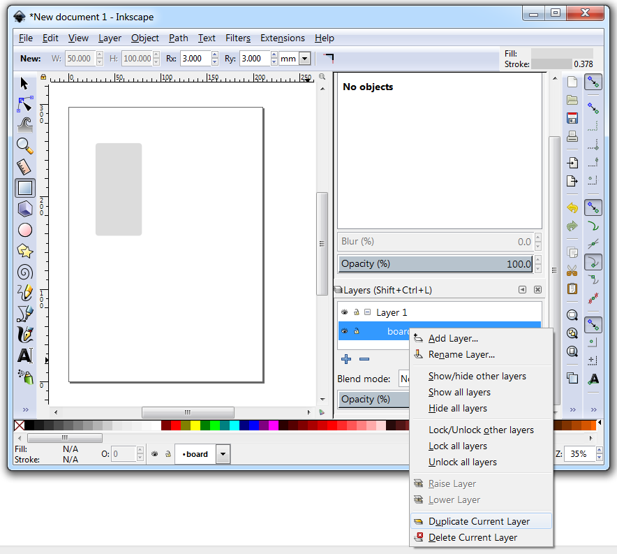
Then, to create the other two, right click the layer named "board" and select Duplicate Current Layer. Do this two times.
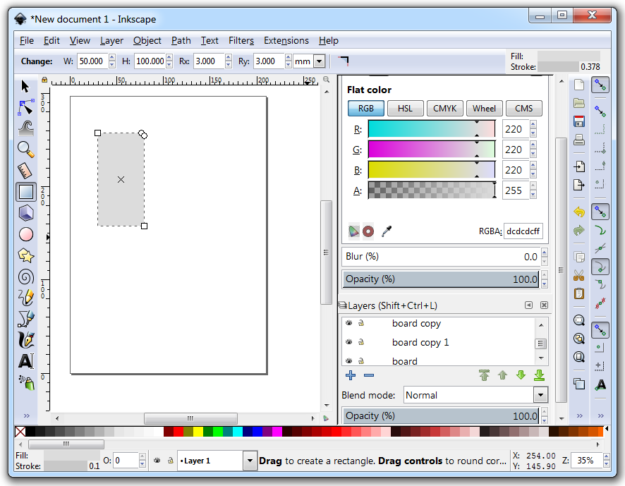
And this is how the layers will look like when done duplicating them.
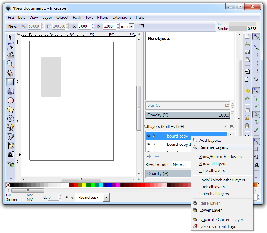
Now right click the copies and rename them silkscreen and silkscreen0
And this is the final state of the layers:
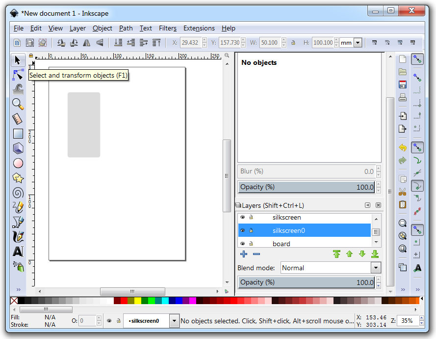
Now, let's move the rectangle to the "board" layer. To do that, click on the Select and Transform Objects tool.
Then click on the rectangle to select it and then right click it. Select Move to Layer...
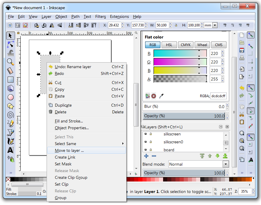
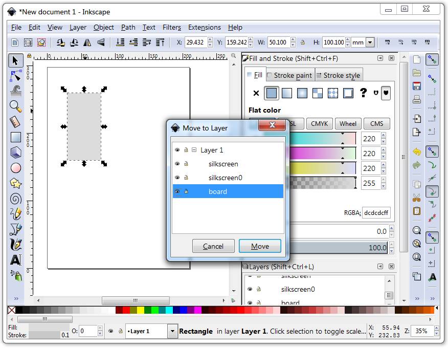
Select the "board" layer to move the rectangle there...
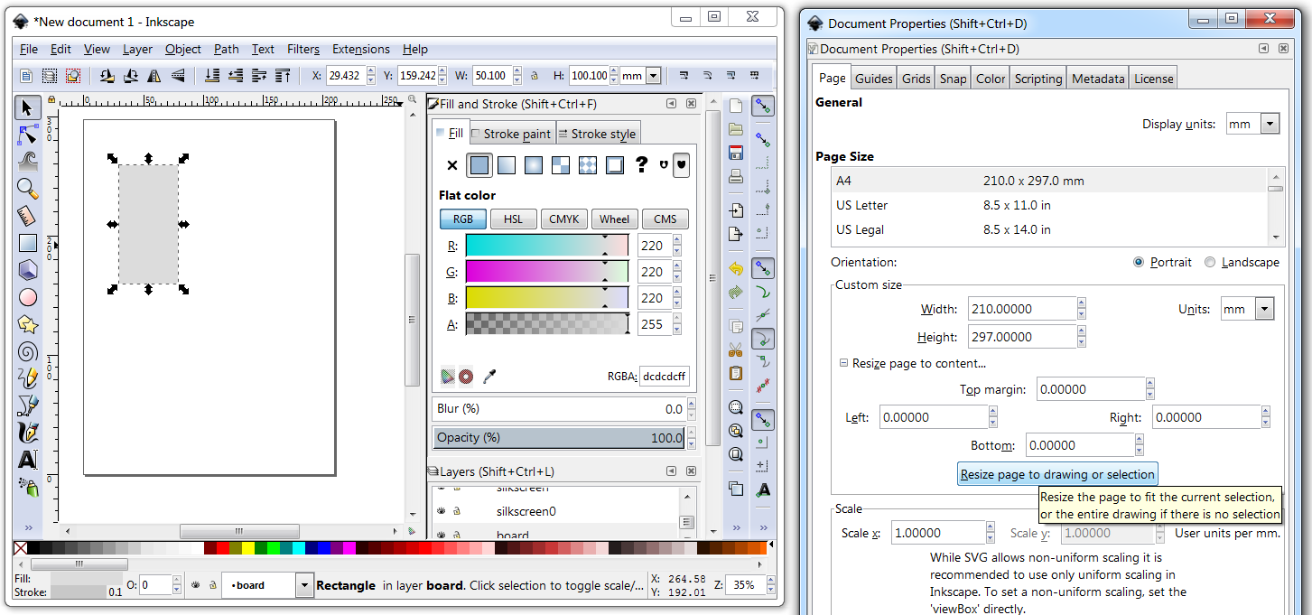
Just one more step before we are done with Inkscape, let's trim the page to the size of the board. To do that, go to File -> Document Properties.
And click on Resize Page to Drawing or section
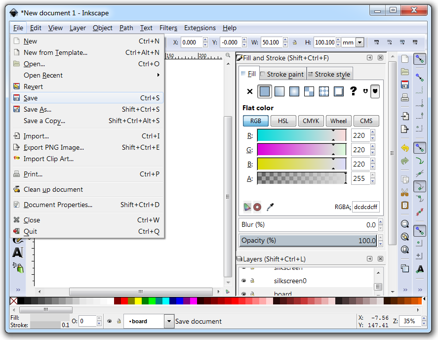
Once the page is shrunk to the size of the rectangle, save the file.
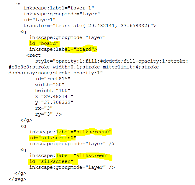
The file, as created by Inkscape, will not work in Fritzing. This is because the layer id property is not set to the names Fritzing expects. The names that we set in Inkscape end up in the label property. I have not found a way to fix this except for editing the file in Wordpad (do not use Notepad as the file does not use the CR LF it expects).
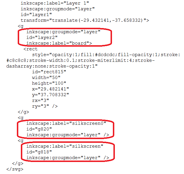
To fix this, once the file is opened in Wordpad, copy the contents of the label property to the id property, as highlighted below.
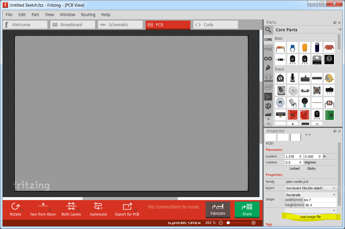
Save the file and launch Fritzing. Click on the PCB and on the inspector window, click on the Load Image File button. Select the SVG file we have been working on.
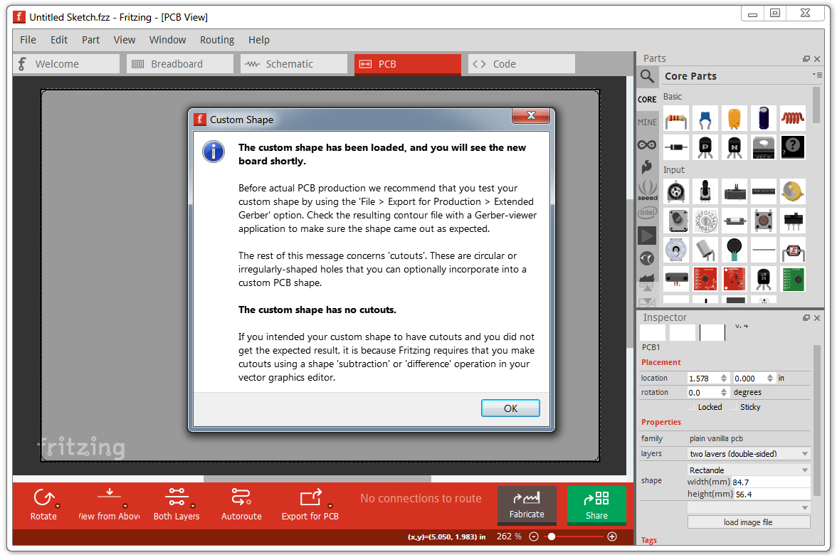
Once Fritzing loads the custom shape it will show the window below. If another window complaining about the lack of a board or a silkscreen appears, go back and double check your work.
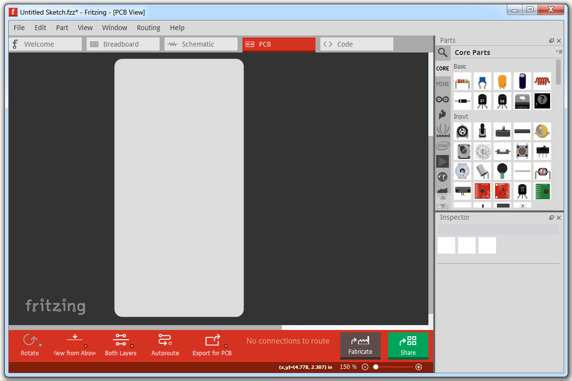
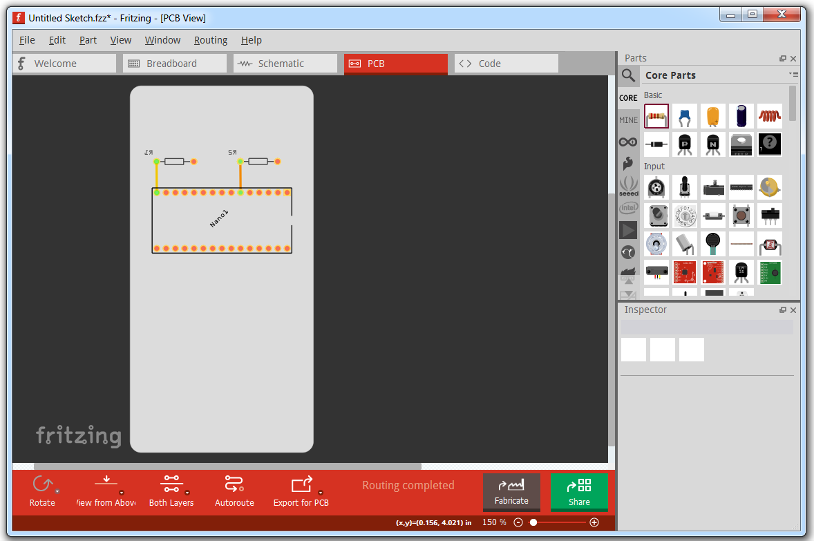
And finally, here is the custom shape loaded in Fritzing, time to place components.
An Arduino Nano was placed as a sanity check to verify our dimensions (50mm width x 100mm height) are correct.
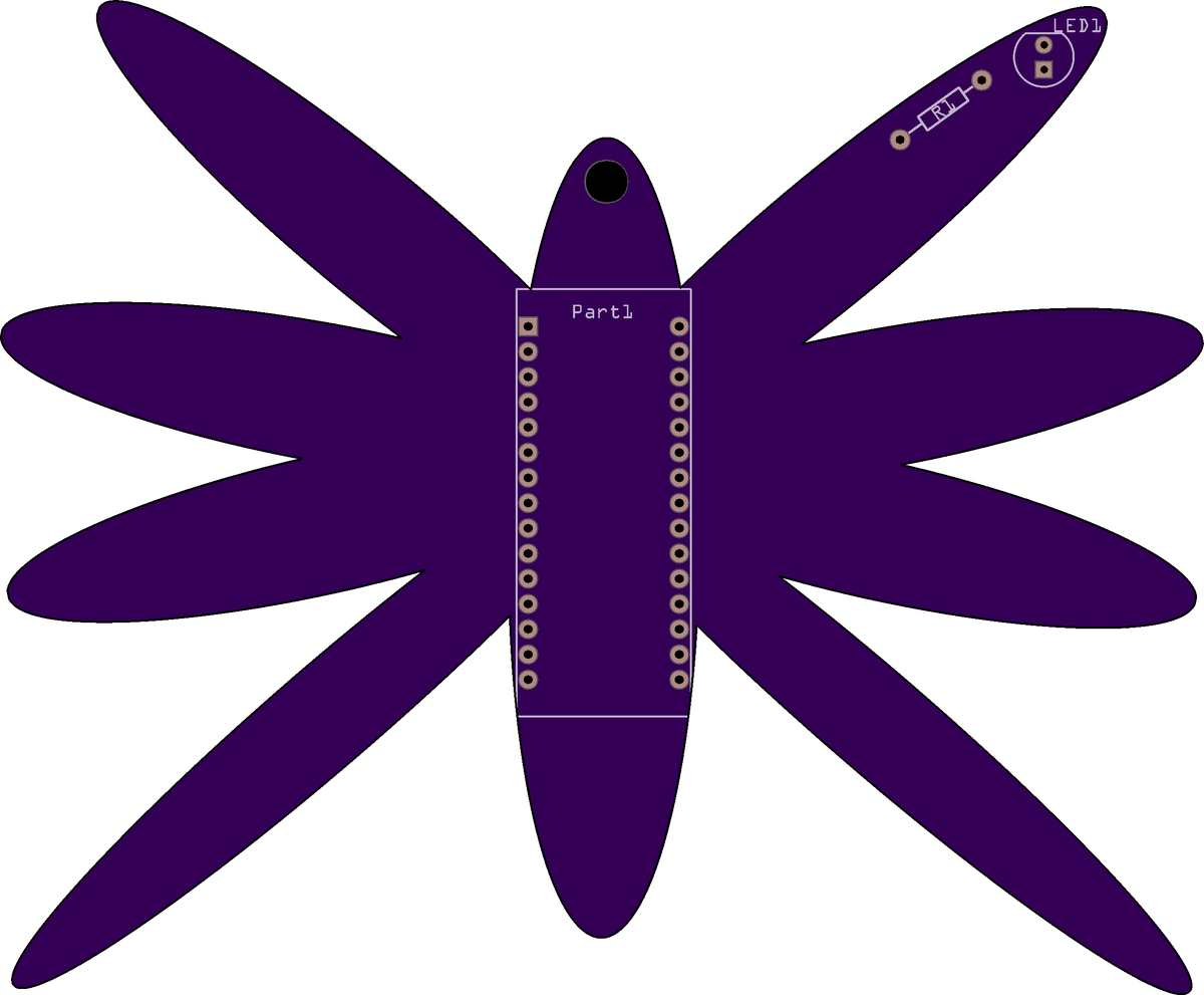
And this is it, If you can draw it, it can be a PCB shape. The shape below was drawn as a series of ovals that were copied, pasted and mirrored, then joined using Union. This unfortunately will not manufacture correctly because the routing bit that will shape it cannot make that sharp bend.
Check out this cool octopus designed by [gsreynaga]. See the inside corners to get an idea what the routing bit can cut correctly.
https://twitter.com/gsreynaga/status/986066660535791616
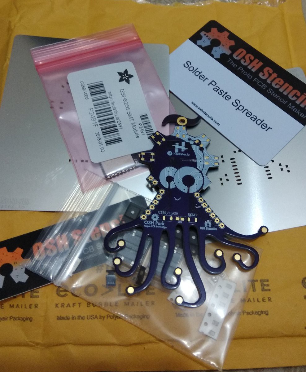
More pictures of the OSHW octopus:
https://www.instagram.com/p/BYHM0vWgilV/
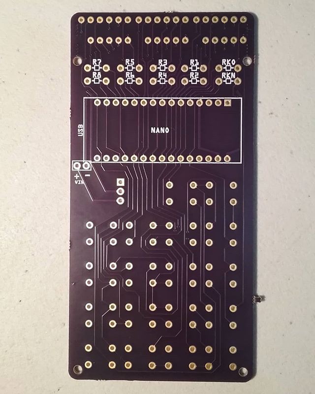
Here is the manufactured PCB, 3mm gives it a subtle rounding effect.
And now hopefully you will never have a PCB with sharp corners anymore.
----
P.S.
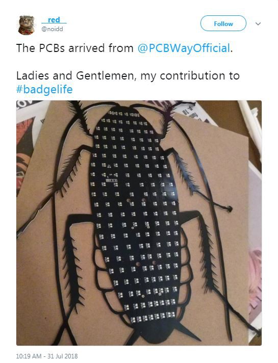
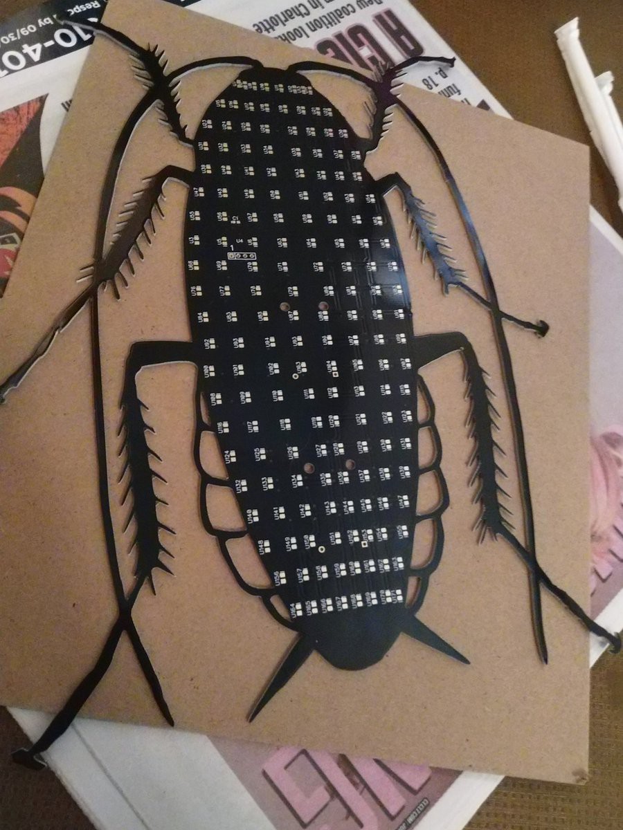
After this log was originally puiblished, the following extremely complex board was found on twitter
https://twitter.com/noidd/status/1024343722933317632
Discussions
Become a Hackaday.io Member
Create an account to leave a comment. Already have an account? Log In.
Nice post. Just FYI, it is possible to edit the Layer ID property within Inkscape directly using the XML Editor option from the Edit menu. I was actually able to design custom shaped boards using Fritzing/Inkscape that way without editing the SVG file directly.
Are you sure? yes | no