 Yann Guidon / YGDES
Once again I got a great result with the batch I submitted to DirtyPCB. This time I chose a larger PCB (100×100mm) to test my idea of a universal module. I could fit 8 10TFF modules in one half of the PCB surface.
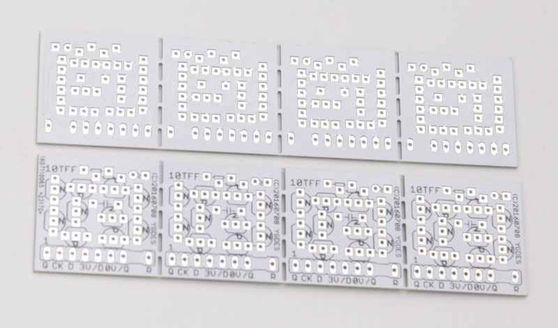
Now I have to solder a few and test them :-)
update 20160804:
It appears that the distance between the pads of the axial capacitor is too short. I modify the component in Eagle to widen the gap and reduce the force on the pins.
The other weird thing is that both types of transistors have a reversed pinout. The BS170s are non-conform and this time, I try the 2N7000 with its reversed pinout. It becomes too complex to plug all the parts in reverse so for this test, I soldered the parts on the other side of the PCB. The outlines still match the parts but on the other side...
Another little change is the resistors values : this time I try with 120K, which should reduce power consumption AND operating frequency, for the slower parts of the clock.
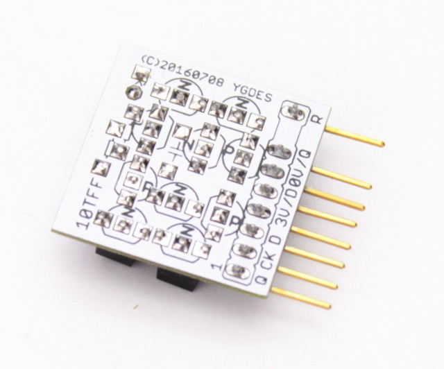
Here is a pretty "usual" module :
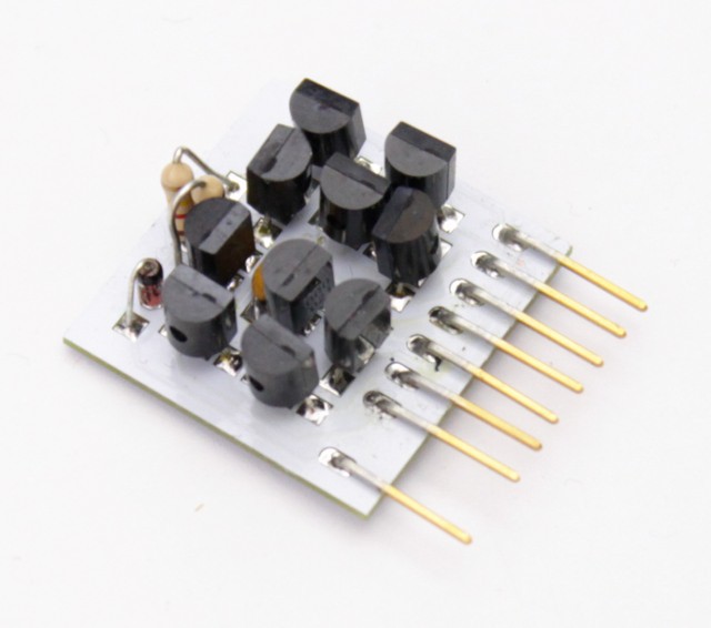
This one is a bit special because the 1N60 diode is connected to the other resistor and resets the latch to the opposite value:
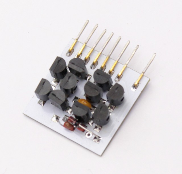
Only one is required in the whole system but it's good to test it. Indeed, I should start to implement and test the mod3, mod5 and mod6 counters...
Discussions
Become a Hackaday.io Member
Create an account to leave a comment. Already have an account? Log In.
Did you panelize this design yourself? If so, can you share what software you used?
Are you sure? yes | no
I used Eagle (6.x). I copied the original layout, then created a blank new PCB and pasted the design several times. Then it's a matter of correct alignment. I think the mill diameter is around 0.8mm and I make 5mm slits with 0.5mm connections. With 0.8mm PCB thickness, this is both solid and breaks away easily. Some sanding is required but not difficult (do not sand after part are soldered or they might be killed by static electricity)
Are you sure? yes | no
OK, thanks!
I guess you have to get the layout correct before the copy/paste, or risk having to do it again. The problem is that my layouts are *never* correct; I can't stop tweaking :-)
I tried gerbmerge a few years ago, and got it to work after some effort, but I'm not convinced it's superior for simpler (e.g. replicate square boards) panelization:
http://microfluidics.utoronto.ca/dropbot/2014/07/30/panelizing-pcbs-with-gerbmerge/
Are you sure? yes | no
The Eagle method is not ideal. But it works reasonably well, if you panelize once in a while...
Are you sure? yes | no