Close
0%
0%

fRISCy: FPGA + RISC-V Digital Processing Board

fRISCy combines SiFive's new RISC-V microcontroller with a Lattice iCE40 FPGA for a platform that is all open source!

Similar projects worth following
Currently, any work with an FPGA will require a proprietary toolchain. Recent advances from Project IceStorm now allow for full Verilog-to-bitstream using open source tools. Combine that with the open RISC-V ISA in the SiFive E310, as well as the SYZYGY open FPGA peripheral connector and you have a high performance platform full of open-source options!

fRISCy could be used in a myriad of ways. First, it can be used for benchtop development work. It would really shine as the central processing unit in a system with different peripherals. For example, it could form the base of a high-performance SDR, or it could be used at the heart of an industrial controls system.

Basic features:
SiFive FE310 RISC-V Microcontroller with 128Mbit QSPI Flash memory
Lattice iCE40 FPGA
SYZYGY Standard carrier-side connector
R-pi form factor including 40-pin GPIO header, RJ-45, and USB Micro-B
10/100 Ethernet PHY
SPI + GPIO interface between FE310 and FPGA for bidirectional data transfer

Hackaday Prize Requirements:

1. Discuss the challenge the project addresses

fRISCy directly addresses the challenge of  designing systems using end-to-end open-source while providing developers with a high-performance platform to design next-generation digital processing solutions for complex systems.

2. Discuss how the project will alleviate or solve the problem that the project addresses

fRISCy offers the following components which allow the use of open-source tools and standards:

Additionally, once complete the fRISCy hardware design files will be released as open-source as well so that anyone can use them. The hardware was developed using open-source tools (KiCad).

3. Publish at least one (1) image illustrating how the project might be used. This may be a sketch, schematic, flow chart, rendering, or other type of image.

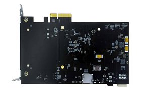
Currently only a block diagram has been uploaded. Hopefully the full schematic will be complete in time to enter this portion of the contest and that will be posted.

4. Link to any repositories (e.g., Github).

https://github.com/shielddigitaldesign/friscy

5. Document all open-source licenses and permissions as well as any applicable third-party licenses/restrictions.

Licenses have not been determined yet.

6. Submit the Project to 2018 Hackaday Prize using the “Submit project to...” option found on the published Project Profile.

Design Justification:

This section will list reasoning behind certain component selections and decisions

  • FPGA: ICE40HX4K-TQ144
    • Biggest motivation to using the iCE40 is the open Project IceStorm toolchain
    • Using TQFP for easier home soldering
    • Also using TQFP vs BGA so that a 4-layer board can be used
      • Original quotes on 6-layer were very expensive
  • MCU: SiFive Freedom E310
    • This part is the original impetus behind the whole project... I got a few of these for free and had to make something with them!
    • Uses the RISC-V architecture
  • SYZYGY peripheral interface
    • Enables more connections and higher speeds than PMOD
    • Less complicated than FMC
    • Open specification
  • 10/100 Ethernet PHY
    • Chosen to operate on the variable SYZYGY IO voltage
    • RMII reduces the number of pins required

Comma-Separated Values - 62.08 kB - 04/23/2018 at 03:13

Download

fRISCy_REV1p1_Schematic.pdf

Rev 1.1 of the schematic. Complete, except a few components need to be updated for Industrial temperature range, and there will probably be some pin-swapping on the FPGA.

Adobe Portable Document Format - 738.85 kB - 04/23/2018 at 03:09

Preview
Download

  • 22APR18: Schematic complete

    Stephen Newberry04/23/2018 at 03:12 0 comments

    I was hoping to have more done by now, but have been very busy. I managed to get a complete schematic uploaded under the "files" section here. There are 2 very minor outstanding items related to the schematic:

    • Pin-swapping will almost certainly change the FPGA pinout during layout
    • There are just a few components that don't meet my goal of having -40C to 85C temperature range. Those will be adjusted.

    A very messy BOM will be uploaded in a minute as well... Not quite complete but getting there!

    -Stephen

  • 16APR18 Update, Power tree diagram added

    Stephen Newberry04/17/2018 at 03:47 0 comments

    As of today, a power tree diagram has been added detailing the power supply input protection, as well as the voltage regulation scheme. The schematic is probably around 80% complete, with the biggest outstanding item being the FTDI device. I'm hoping to be able to use the FTDI for multiple functions: JTAG to RISC-V MCU, SPI for configuration of the FPGA, a UART to the FPGA (if we need to connect to the RISC-V UART, we can just set up a pass-thru in the FPGA). I'm hoping that the SPI interface between the FTDI and the FPGA can be used as a data transfer port as well, after the FPGA has been configured. All of the IO pins to the FPGA have been assigned on the schematic, but I will go through the process of pin-swapping during layout. I don't think I'll make the deadline for schematic completion by the time the Hackaday prize entry date comes, but I will certainly continue to work on the project even after the deadline. I plan to release the design files to a public repository under an OSHW license once the design is complete as well.

    -Stephen

  • 20MAR18 Update, Initial publication on hackaday.io

    Stephen Newberry03/21/2018 at 00:01 0 comments

    20MAR18:

    Original publish date on hackaday.io. At this point, the Artix-7 has been removed from the schematic, and the iCE40 has been added. Complete connection details on the iCE40 need to be added. Some component selection is still necessary (notably, what type of external memory to use on the FPGA). Additionally, the programming interface still needs design and validation.

    The fRISCy schematic is approximately 70% complete, and PCB layout is approximately 40% complete. Design documentation needs to be generated as well, including:

    • Updated system block diagram
    • Clock and Reset block diagram
    • Power distribution tree

    Upon completion of the schematic, the following files will be generated:

    • PDF of schematic
    • BOM
    • Component operating temperature range report

    Upon completion of the PCB layout, the following files will be generated:

    • Fabrication files:
      • Gerbers
      • Drill
      • Pick/place

View all 3 project logs

Enjoy this project?

Share

Discussions

rich wrote 08/29/2019 at 16:31 point

Just what I need. Is the project alive?

Any interest in a board build?

  Are you sure? yes | no

Martin Cejp wrote 04/25/2018 at 18:21 point

Really looking forward to this. Freedom is the future!

  Are you sure? yes | no

pagercam wrote 03/29/2018 at 19:32 point

As you are using the TQ144 footprint anyway you might as well use the

ICE40HX4K-TQ144

Same footprint, only $1.26 more on Digikey, part is labeled as 4K and can only use 4K size in Lattice tools but using Icestorm you will find that it is really an 8K part and can be used as such.  Remember you can never have too many friends, money or LUTS/FF!!!


  Are you sure? yes | no

Stephen Newberry wrote 03/29/2018 at 19:46 point

Absolutely right! (at least the LUTS part :) It's already been changed in the schematic but I haven't gotten a chance to update this page yet.

  Are you sure? yes | no

Similar Projects

Does this project spark your interest?

Become a member to follow this project and never miss any updates