 Grant Giesbrecht
The computer uses flash memory to store its programs and save data. Earlier I made the mistake of trying to write to flash memory the same way I did for SRAM - by entering a value on the data and address lines and pulsing write_enable low. I should have RTFM because it is, of course, much more complicated than that. For those of you who aren't intimately familiar with flash chips (as I wasn't), they have a couple of peculiarities which makes them challenging to use (especially compared to reading/writing SRAM, which tends to be more straight-forward). For one, they are often protected by software data protection. This means to erase or overwrite data you must first enter a series of codes on the data and address lines. This prevents the chip from being inadvertently deleted or corrupted, especially during power up and power down. Another peculiarity is a consequence of how flash works physically and is that when you write to flash you can typically only 'set' a bit, but not 'reset' it (ie. you can change it from 1->0, but you can't change it back to 1 without erasing the entire sector). This brings me to the last quirk - sector erase. Flash has to be erased in sectors. For some chips, this means to reset a single bit back to 1 you have reset every bit in the entire chip back to 1s! - Moral of the story: any homebrew flash memory controller will need to support software data protection and be able to erase and write in sectors.
I decided to buy flash that allowed me to erase sectors that were smaller than in the first chip I tried (4kB instead of the 128kB entire chip). After I settled on a specific flash model, I set about designing a controller for the chip. The duties performed by the flash memory controller (FMC) include:
- entering software data protection codes
- Controlling timing of memory registers
I settled on a design that used registers to hold the address and data values to read/write so that I could free up pins on the microcontroller which would run the FMC. One big hurdle was devising a way to get the software data protection (SDP) codes entered while not taking up 24 pins (8 for data byte, 16 for address bytes) on the MCU. I noticed that only a few values are used in all of the SDP sequences, so I elected to use a network of logic gates controlled by only a few pins to generate the 24 bits needed for the SDP codes. To write or read to the chip, the address is entered into two 8-bit registers via the computer's main bus, the data (if it's a write operation) is entered into a 3rd 8-bit register, and the FMC takes over entering the necessary SDP codes and timing to complete the operation. An operation is requested by specifying the type of operation (read, write, sector erase, chip erase) on two lines, then triggering interrupt 0 of the AVR MCU.
I prototyped my design on four breadboards and worked out a few kinks in the hardware. I wrote a C program for the AVR MCU and tested it on the FMC and got the program working. Here's a shot of the prototype:
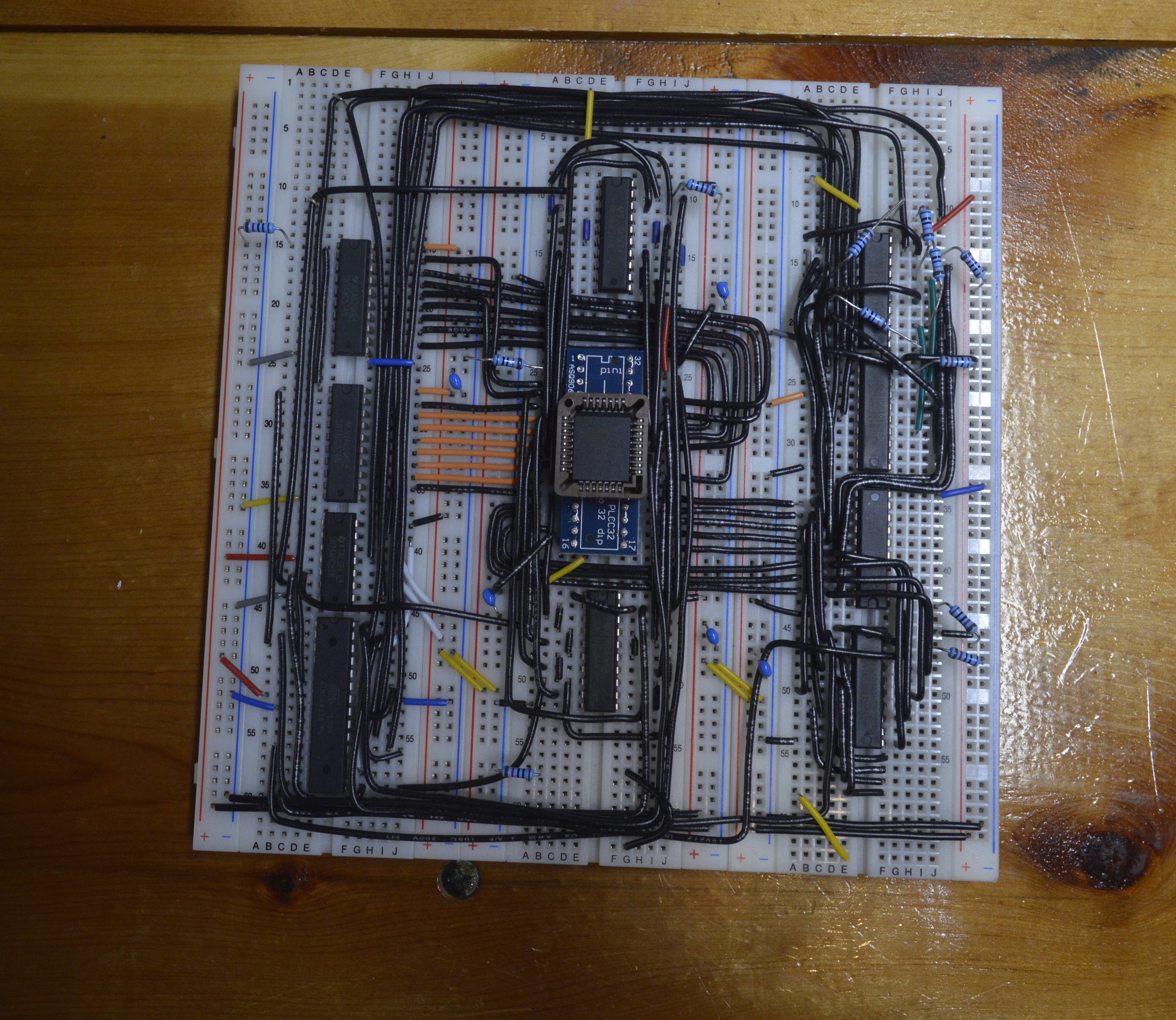
This was definitely one of the more complicated modules in the computer. It took me forever to get right because I kept trying to jump right in to building it before actually having a comprehensive plan. After numerous failed attempts I finally committed to carefully re-reading the datasheet and drafting a few different plans. I considered doing everything with microcontrollers but decided that wouldn't work as well as what I settled on - using one micro to synchronize a whole bunch of 74-series chips.
If anyone wants to build their own homebrew computer with flash memory, you might consider copying my design. I'm confident it's not the best solution but it does work (err, it works right now. I suppose I can't really claim it works until the whole machine is done). It was a pretty tedious part to get through so taking a short cut here might be worth while.
Discussions
Become a Hackaday.io Member
Create an account to leave a comment. Already have an account? Log In.