 Ziv Barcesat
Create and build your own business card on a PCB with NFC capability
Step 1: Design your PCB
you would need to design your PCB to include your contact details, graphics and also select the dimensions of the card.
You can use my example by opening it using EasyEDA Standard to import the schematic and PCB json files or clone it from this project on OSHWLAB
I have also cloned the project at first from this one. Shoutout to CoolCoderSJ!
Step 2: Manufacture your PCB
I have used JLCPCB to manufacture the PCBs, it was easy to do and the results look great (they even remade part of the batch because they found scratches on some of the boards, so I got more boards eventually).
Here are the parameters I've used:
- Base Material: FR-4
- Layers: 2
- Dimension: 88.9 mm* 50.8 mm
- Product Type: Industrial/Consumer electronics
- Different Design: 1
- Delivery Format: Single PCB
- PCB Thickness: 0.6
- Impedance Control: no
- PCB Color: Green
- Silkscreen: White
- Material Type: FR4-Standard TG 135-140
- Via Covering: Tented
- Surface Finish: ENIG
- Gold Fingers: 1U"
- Deburring/Edge rounding: No
- Outer Copper Weight: 1 oz
- Gold Fingers: No
- Flying Probe Test: Fully Test
- Castellated Holes: no
- Edge Plating: No
- Remove Order Number: Yes
- 4-Wire Kelvin Test: No
- Paper between PCBs: No
- Appearance Quality: IPC Class 2 Standard
- Silkscreen Technology: Ink-jet/Screen Printing Silkscreen
- Package Box: With JLCPCB logo
- Board Outline Tolerance: ±0.2mm(Regular)
One thing that I would like to think about for the next order is to also order a stencil since it makes the boards easier to assemble. A thing to note is, that if you've designed visible copper traces such as your name, they would be exposed in the stencil. In ordr to avoid that you'd need to review or design the stencil yourself.
Here are the manufactured PCBs:
Step 3: Order parts
To assemble the board, you would need these parts (Digikey links):
1. 1K memory NFC chip with I2C Interface
2. 0.22 uF Capacitor
3. 47 Ohm Resistor
4. Red LED
To assemble the board you would need some kind of a solder paste like this one
Step 4: Assemble your board
The required tools are:
1. A hot plate or a hot air gun
2. A soldering Iron
3. A solder wick
4. tweezers to place tiny parts on the board
5. Some kind of a magnifying lens or microscope
Assembly steps:
1. Spread a thin layer of solder paste on the component pads.
2. Carefully pick and place the components on the board.
3. Align the parts in their correct orientation (Specifically, the NFC chip and the LED)
4. Solder the components in place (I have used a hot plate), look out for flying bits and deformation of the PCB due to the temperature difference.
5. Perform visual inspection on the boards (As you can see, I had a lot of shorts that would be easily cleaned with solder wick)
Here is the assembled PCB:
Step 5: Program your board
I have used at first an arduino micro and after that moved to an esp32 dev board to program the boards.
In order to connect to them, I first used wirewrap wires and after that used PCBite needle probes. There are 4 connections that need to be made:
1. VCC to 3.3V
2. GND to GND
3. SCL to SCL (I2C interface)
4. SDA to SDA (I2C interface)
I have used the code from this repository as a base to check the connections
to run the tag provisioning code, open the Platformio project that's found in here.
This code scans for the tag using I2C in the default adderss 0x55, deletes the memory and read the registers to validate and check the chip.
After that the code will run for a loop and will report if a field is found (aka the tag is read with a NFC reader or a phone).
To perform the initialization on a series of tags, simply connect the programming board to the tag and hit the reset button. Then, reconnect the next tag, hit reset, etc.
Step 6: Write NFC records
I have used NFC Tools to read the tag, create a contact URI record, and write it to the tag!
#TODO: add screenshots


 Lithium ION
 DIY GUY Chris
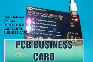
 Michael Delaney
please make CC1101 and ruby or python embeded