 Colin O'Flynn
Links to project details (GIT, Wiki, Docs) are on the left. The laziest intro to this project is the 2-minuite video created for THP Quarterfinals (i.e. the first video I made):
Or even better, see my full 5-min final video (there is also the semifinal video, see link at left):
The most commitment is reading this page! Well if you are still reading, strap yourself in...
What's This About?
Lots of people have tried to design secure systems, and alas there is lots of failures. But what if you did everything correct: no buffer overflows, no unsanitized inputs, no default passwords. Unfortunately this isn't good enough - even perfectly implemented encryption algorithms such as AES-256 will reveal encryption keys. It's not due to incorrect implementation, it's a fundamental artifact of the design.
This has been known for a long time - the first paper on this was published in 1998. But if you are an engineer or independent researcher tools to get started are expensive, or require you to do a lot of work yourself scripting together lower-cost tools. This project is my attempt to eliminate this problem.
I'm eliminating the problem for good by making my tools open source. Because this whole area is an active research area, the tools need to be open source. This isn't a case of attempting to seem sexy by adding the word 'open-source', but placing something of commercial value into the open-source domain, in the hope it spurs a larger community. Think of something like Wireshark - it's extremely valuable, and could easily be sold as a high-end product. But most of that value comes from it being open source, and hence containing a huge array of protocol dissectors, far beyond what a commercial vendor could support. For my designs, part of the larger community includes hours of tutorials on this area - the objective of ChipWhisperer is not just the engineering that went into the software and hardware, but having tutorials and documentation that could be used as a complete course in side-channel analysis and glitching.
It's also worth stressing that there is no 'tricks' to the open-source nature of this project. It's not just part of the design that's open source, I'm not using a restrictive non-commercial license, and I've already had other people build these units from PCB design files. The objective of this is project is to open up this area of research to a much wider audience, and the commercial value I lose from limiting how much I can charge for the tools (since anyone can make them) is far offset by the greater value added to the community.

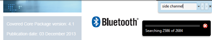
It's useful to point out how critical this field of embedded security has become, and why it's interesting to see attacks against AES (which I tend to focus on in my demos). The 'Internet of Things' requires some wireless communication network - be it IEEE 802.15.4, ZigBee (which uses 802.15.4), or Bluetooth Low Energy. Since these are wireless protocols, security is of paramount importance - and the designers acknowledge that. Attacks against AES are interesting because all three of the previous protocols use AES-128 for security. Unfortunately AES-128 isn't just a "check box" that indicates your system is secure, despite one document listing that because Bluetooth low energy has 128 bit AES, it's "secure against attack and hacking" (see page 45). The idea that implementations are secure because the underlying algorithm is secure will cost somebody a lot of money when it blows up in their face, and they have to fix millions of already deployed devices.
Assuming designers aren't foolish enough to send encryption keys over SPI (see Travis Goodspeed's attacks), and have actually done the implementation correctly, and haven't introduced backdoors, we can still break the AES implementation. This isn't a theoretical attack, but a real-world attack that every embedded designer needs to understand. It's clear that very few designers are aware of this issue, based on how infrequently it is brought up when looking over datasheets, design specifications, and application notes. And no, it's not enough to use hardware accelerators - an attack has been demonstrated against the XMEGA crypto engine (presentation slides, details on page 77 of thesis, article at ACM behind paywall). See the 2684 pages of Bluetooth specification for example, not a hit for 'side channel' to be found:
ChipWhisperer won't secure the internet of things. But it will hopefully jolt people into believing that "secure because math" isn't a good enough answer. Even these theoretically unbreakable cryptographic algorithms have great weaknesses during implementation, and they may be much easier to break than you ever assumed. So let's start looking into how this works.

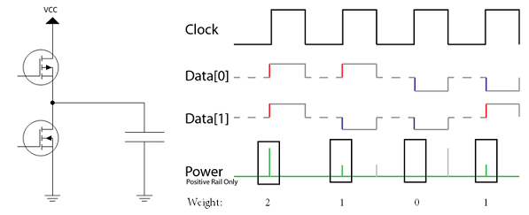
Side channel analysis takes advantage of the fact that changing the state of a digital line uses a small amount of power. Switching from a 'zero' to a 'one' takes a small charge for example. Many digital ICs will also push the lines into a 'pre-charge' state in-between transitions to reduce the worst-case time delay, such that on every cycle the bus goes from an intermediate state to a final state. For us this means we can almost directly infer the Hamming Weight (number of one's) on a digital bus based on the power consumption.
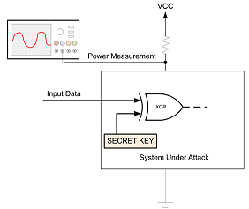
So what does that give us? Consider that we had the following system, which is a simple XOR of some input data with a secret key, where we don't see the final output:
While we can build the following matrix, given some known inputs, along with the associated hamming weights based on the power measurement:
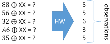
Then one can simply guess what the secret key was! Based on our guess we can determine which guess best aligns with the real measurements. In the following example if the secret key was 0xEF, we would end up with the hamming weight matching our observations:
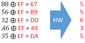
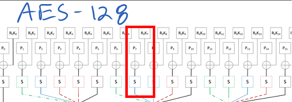
Finally, the reason this works so well is that it allows us to break a single byte of the encryption key at a time! Thus the minimal guess-and check means guessing 256 possibilities for each byte, and doing that 16 times:
For more details see my write-up on the theory of a CPA attack, along with a nice example of step-by-step breaking of the AES using Python from my ChipWhisperer tutorial list. For the attack to work, we basically just need to be able to tell the encryption/decryption algorithm to operate while we monitor the power, and know either the output or input to the system.
This can be done with ~20 power traces on an AVR device for example, so it's not a case of taking an unrealistic number of measurements. For example see a real-time example of me breaking an AES-128 implementation in 120 seconds.

Glitching is another devious attack on embedded systems. This takes advantage of the fact that at some point in your code you'll have a test of the input password, signature, or whatever else. So consider we have this code:
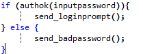
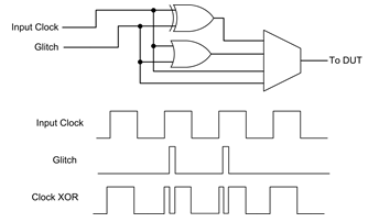
It's actually possible to manipulate the system to cause that check to fail, or for instructions to be skipped. One method of doing this is inserting a quick glitch into the clock, as the following example from the ChipWhisperer shows:
This "double-edge" causes timing errors in the target device. The result of this varies, but often results in an instruction skip or the wrong result of a comparison to be loaded. As an example see my video showing clock glitching breaking a password check.
If you are looking for some additional detail see the full ChipWhisperer clock glitching tutorial, which includes a 35 minute video tutorial.
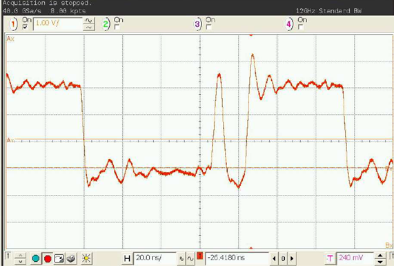
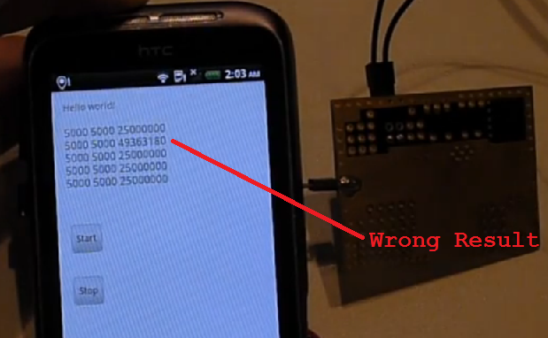
Even somewhat more interesting, is the fact you can do this with 'power glitching'. This means inserting some sort of low-voltage spike into the VCC line of the device you are targetting. This works even for advanced chips, like a Raspberry Pi or Android Smartphone. The VCC line glitch might look like this:
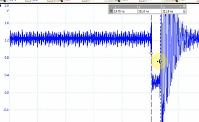
This can cause a user-land application to fail on something like an Android smartphone - here is an example where I'm causing an incorrect calculation, this example comes from my project log update:
There is a full ChipWhisperer VCC glitching tutorial which targets an AVR microcontroller, in the same fashion as the clock glitching tutorial. Now that you get an idea of why these attacks are so interesting, let's look at what ChipWhisperer can do.

The system is a fusion of closely operating FPGA blocks and a Python interface communicating over a high-speed USB 2.0 interface. It even uses partial reconfiguration to reprogram the Spartan 6 FPGA during operation to fine-tune certain parameters that would otherwise be fixed when implementing the FPGA. Remote database storage of traces is used to power high-performance analysis, levelling the playing field for the independent researcher who doesn't have access to costly computing hardware.
Having the computer connectivity of the hardware is fundamental to the operation of this device. In addition it's possible (and sometimes required) to have the device split over several locations via a network. This can mean the ChipWhisperer is running on one computer, with data being saved to a larger network store. Even for researchers who do have local access to a high-performance computer, the remote storage is often useful, since the physical attack may be occurring at a different spot from the analysis computer.
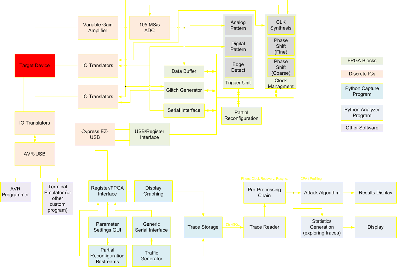
The blocks themselves can be implemented into many different FPGAs - this system is not limited to the capture hardware created as part of this project.

This project has spawned a number of useful modules, some of which are already being used in other open source projects. The following section briefly summarizes some of the hardware modules, software modules, and techniques which I created for ChipWhisperer (but are useful for a variety of open-source projects).
Synchronous Sampling: The synchronization of the sample clock to the device clock fundamentally differentiates the ChipWhisperer from commercial solutions, even the extremely expensive ones. This allows the ChipWhisperer to break systems that would otherwise require 5GS/s or faster oscilloscopes according to published academic papers. Currently the ChipWhisperer is the only solution (commercial or otherwise) using synchronous sampling with variable phase offset, allowing it to attack devices with internal oscillators or with varying-clock countermeasures. The use of Synchronous Sampling is the basis for three academic papers (including a journal article), demonstrating the innovation of this technique. More details will be presented later.
OpenADC: The OpenADC was the first module created, and is the high-speed ADC block. In addition I've published the FPGA code for storing samples and downloading those samples to the computer via Python. Besides my academic papers using the OpenADC, I've found a few other papers (1, 2, 3) using the OpenADC for doing research into low-power wireless networks and crypto. It's extremely exciting to see my work being used already! More details of the OpenADC are given later in this description.
PyQtGraph Parameter Tree Updates: This project uses PyQtGraph for both graphing along with setting of parameters for almost the entire project. This involved some updates to the PyQtGraph implementations, specifically the ability of setting parameters to automatically download them to the hardware, and verify the setting in hardware.
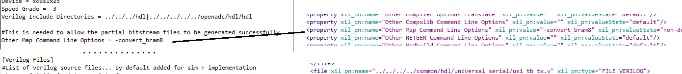
FPGA Project File Generation: The Xilinx ISE Project navigator files are an XML based format, but have a serious problem when attempting to commit them to GIT: they change for every version of ISE! In addition you need different project files for each FPGA device supported. This causes many headaches: commit conflicts for different versions, along with maintaining multiple files for each project. ChipWhisperer uses a simple text file to automatically generate both the ISE Project file and associated COREGen files, see details in the log post.
FPGA SAD Trigger: The Sum of Absolute Difference (SAD) trigger FPGA block performs real-time pattern matching of a stored pattern to the incoming waveform. This means the pattern matching runs at the ADC speed (i.e. 105MS/s), and was successfully implemented in a low-cost (i.e. fairly slow) Spartan 6 FPGA. This would be trivial to do in software, but unacceptably slow and with jitter relative to the device clock. The FPGA block is able to detect a match exactly six sample clocks after the final sample of the pattern being digitized. More details of this are presented later.
FPGA Dynamic Clock Blocks: FPGAs provide various blocks for clock control, but typically expose a fairly complex interface. As part of my project I designed several modules that simplify this interface, allowing you to access the dynamic phase shift and dynamic frequency generation blocks. There is even Python code for automatically configuring the blocks given a desired output frequency for example, and the proper parameters are dynamically downloaded to the blocks. In addition this system supports an advanced feature called Partial Reconfiguration to allow you to dynamically tune all features of the clock module blocks, even a number that according to Xilinx are fixed at design-time.
FPGA USB Interface: A classic problem in FPGA designs is where one needs to control a few registers from a computer. I designed my own interface for this, which can run on almost any other FPGA development board, provides the ability to almost max out high-speed USB when downloading data, and has a simple Python interface. More details of this are presented later.
Waveform Plotting: The ChipWhisperer requires high-speed plotting of many waveforms. This is primarily handled by the PyQtGraph library, but that library has been extended to support additional features such as a dock with a toolbar for accessing various plot functions. Like most of the ChipWhisperers source it's all very modular, meaning you can rip that waveform display code out for something else.

When starting this project, it was destined to be open source. ChipWhisperer does not aim to be just a complete tool, but also a useful platform for further research. For example I assume 99.5% of users will never modify the FPGA code, and couldn't care that it's open source. But there is still that 0.5% - and the value of the open-source code to that 0.5% is what makes it worthwhile. So who are the 0.5%? I assume they would mostly be researchers; the area of embedded hardware security is an extremely active research area. There's a number of conferences and journals in this area, and researchers in this area are no strangers to FPGA work, or even designing custom chips. For that 0.5% of users, this project could save them from months to years of work (since they don't need to redo my work).
The core Python code is more likely to be modified (since it requires less effort than the FPGA design), but even then I've tried to make it as easy to 'hack in' extra modules as possible. I know from experience that of those that DO wish to modify the code, they will mostly want to get something working quickly. This is part of the reason the code supports all sorts of dynamic Python execution and loading of external modules (discussed in detail later).
By sharing the ChipWhisperer design, it provides a useful starting point for these researchers to build upon. If you decided to work on a real-time analysis algorithm implemented in an FPGA, the ChipWhisperer would be a perfect platform for your work. In addition the platform is commercially available, meaning that when researchers disseminate results based on the ChipWhisperer, it's trivial for someone else to duplicate or verify the results.
I've already received feedback from people using portions of this project. The ADC board (OpenADC) has been used in a number of other projects, and I've even had people in other countries thank me for providing the designs, as it's difficult for them to import PCBs in their country. But since they had the design files, they could have them made locally without issue.
Having previous experience with open-source projects, I'm familiar with many of the issues that hit these projects. In particular documentation is often a problem. Documentation doesn't seem as sexy as hard-core engineering, but unless the project is well documented it has zero hope of continuing once the main developer moves on or is hit by a bus. ChipWhisperer has a massive documentation repository, and it's still growing as this project is in it's infancy! Let's look at that next.

There are several main sources of documentation:
- Full Project Documentation: This is the major documentation, and includes both python API documentation, along with detailed instructions for installing python modules, using the hardware, etc. This documentation aims to be a polished resource.
- The Wiki: The wiki contains additional detail such as most recent releases, instructions for building hardware, BOMs, various small notes, and example traces. This aims to be a 'living' documentation so is subject to frequent changes, and has many short and simple pages such as PCB errata.
- Presentations & Whitepapers: There are a number of presentations I've previously given. The link to the left includes a few of the earlier Blackhat presentations, which have a long whitepaper too!
- Videos: I've got several hours of video tutorials. See the full list later on in the 'video' section of this document.
- The GIT Repository: Some people believe code is self-documenting. I've tried to help it along with docstrings and whatnot, but the GIT repository is the ultimate source for all things about this project.
Here's a few pictures of the documentation:

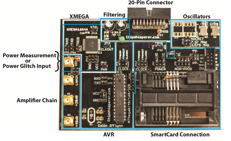
Some of the blocks on the main PCB are shown below. The OpenADC is my open-source ADC board which was designed as part of this project. The rest of the chips have various glue logic for easing interface to the FPGA, and a USB-connected AVR for 'additional stuff'. This can mean using it to program a target, talking some specific protocol, etc.
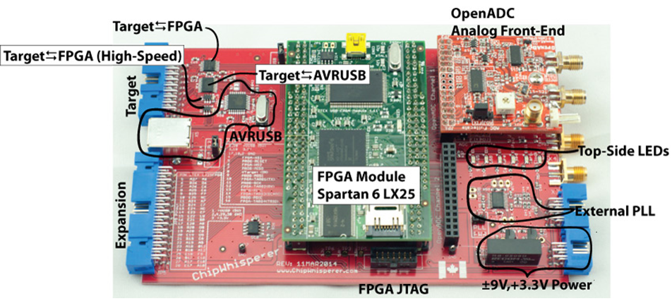
Target IO Interface
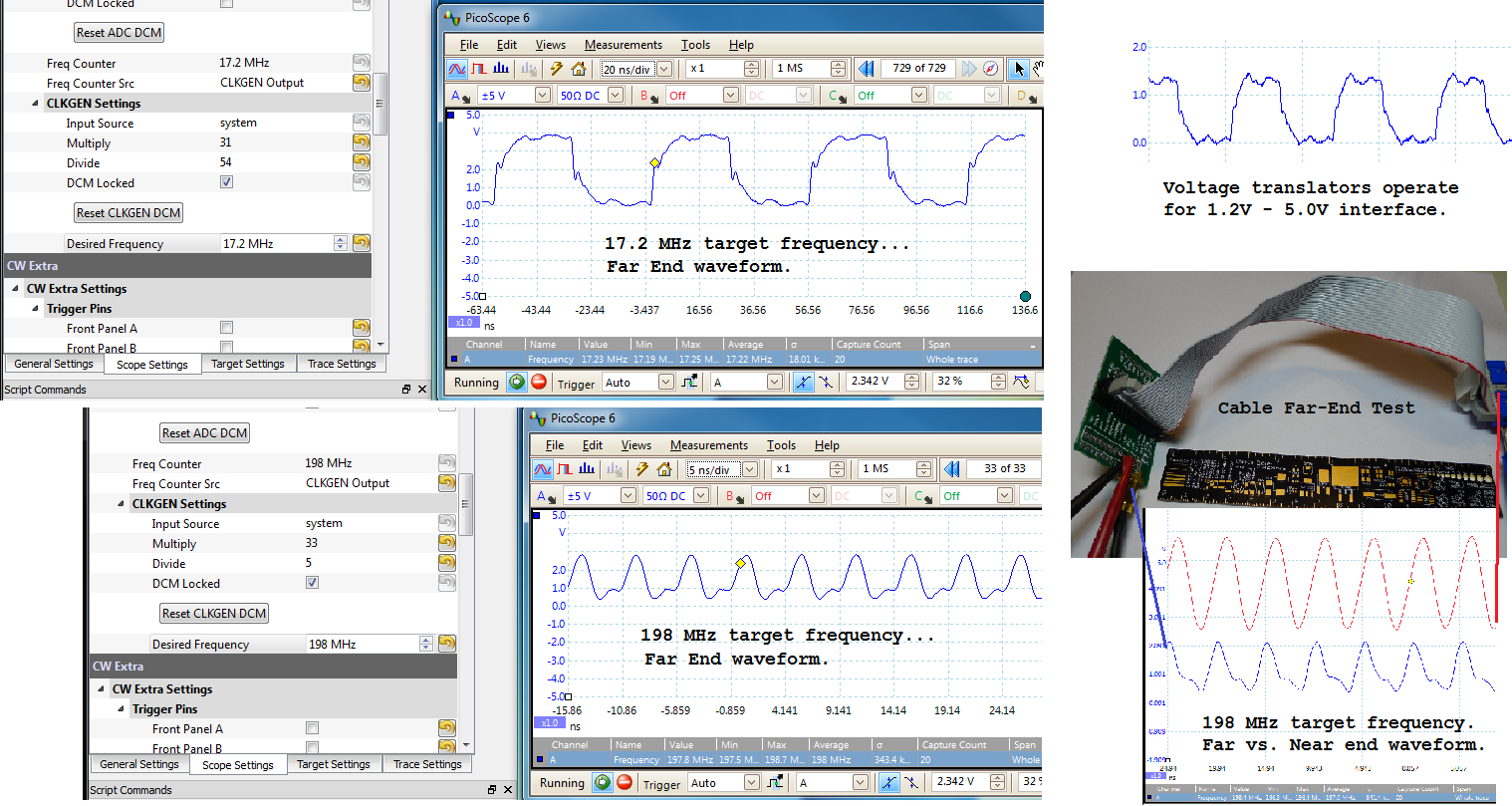
Twelve IO lines pass through level translators for use in a connection to the target device. Two of them use high-speed translators, which can be used for generating a clock to the target device, triggering a glitch, or receiving a clock from the target device. The ChipWhisperer can even be used as a simple clock generator for digital devices too - from the GUI a requested clock frequency is automatically generated by the internal clock module. Normally the output is fed over a standard ribbon cable. While not an impedance matched connector, for many experiments this performs 'well enough' in practice. The following shows some figures after 8 inches of ribbon cable. Note the 'near end' waveform taken at the back-side of the connector for the 198 MHz test frequency shows less duty cycle distortion compared to the far end waveform. This suggests using a shorter cable or designing a breakout board to plug into the header with SMA cables might be successful for high frequencies to reduce duty cycle distortion. The oscilloscope used in these tests had a 350 MHz analog bandwidth, meaning the 198 MHz waveforms don't have all the detail present (overshoot/undershoot + edges attenuated severely).
AVR-USB Connection
The AVR-USB connection is an AT90USB162 device. It can be programmed with a AVR-ISP MK2 clone firmware from the LUFA project, or can be programmed with other interface code such as my example USB-SPI driver. This allows for a complete development system, since you can use this device to program new cryptographic code into the device being tested.
FPGA Module Power Supplies
Originally, I wasn't sure if the LX25 FPGA would be powerful enough, so the system was designed to accept larger FPGA modules with everything up to a Spartan 6 LX150. These larger FPGAs require higher current sourcing capabilities, so the supplies were originally designed to meet these higher current limits.
As an example the 2.5V rail is being tested with an electronically switched (via a relay) load in the following figures. Some contact bounce of the relay can be seen, but notice there is little change in the noise on the supply rail even at these high currents.
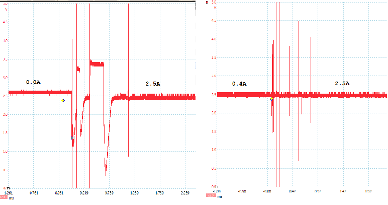
Details of the test jig are shown in my project log update.
External PLL
Due to limits in the FPGA clock blocks, an external PLL is also present. Whereas the Spartan 6 clock blocks are spec'd down to an input frequency of ~5MHz, the external PLL chip can operate down to ~1MHz. This allows an extended input frequency range, in addition to providing a LVDS input path for the clock.
Multi-Target Victim Board
The multi-target victim board is a simple demonstration platform. This can be programmed with various cryptographic algorithms, and provides the ability to monitor power consumption and insert clock glitches. It can be used stand-alone with a normal oscilloscope (i.e. it is not tied to the ChipWhisperer Capture hardware) because of the Low Noise Amplifiers which can boost the small signals to levels a regular oscilloscope can measure.
OpenADC
The OpenADC board is a modular ADC board. It uses the 'PMOD' connectors which are supported by a bunch of FPGA boards, especially those from Digilent. It's been designed to be fairly low-noise, and I've had a lot of positive feedback from that design! It's a simple 2-layer board, although it's been carefully routed such that the bottom layer is almost entirely ground plane, check it out:

There's no separate analog/digital ground, instead the layout tries to keep the analog and digital portions separated such that digital ground currents won't flow over the analog portions. I'd love to hear your feedback, but it seemed in my research that separating them can add issues with ground loops when the separation isn't 100% perfect (i.e. you run a digital trace over the analog ground, causing the digital return current to take a much longer path than it would have with a single plane).
The 3.0V analog supply for the ADC comes from an on-board LDO regulator, which filters the 3.3V input supply. The LNA chip required a 5.0V supply so there is also a 3.3V to 5.0V switched-capacitor based DC-DC on board. You'll see a number of ferrite beads (look at the Lx parts) that form supply filters.
The OpenADC has already been used in other academic publications beside my own. I have no connection with the following authors, I happen to discover their paper while searching my own references: (1),(2),(3).
Links to Schematics, Gerbers, BOM, Assembly Instructions
Everything is done with 2-layer PCBs to keep cost down. The following is a list of most of the hardware design files involved in this project, although see the GIT repository for full project design files, including beta/incomplete boards. Some of the links go to the GIT repo, and you have to hit the "Download" link to get a .zip of that folder.
The following are the "core" files which are used to build the ChipWhisperer Capture Rev2:
OpenADC: PCB Gerbers, Assembly Instructions/BOM, Schematic (PDF), Eagle Files, Datasheet with User Guide
ChipWhisperer Baseboard: PCB Gerbers, Assembly Instructions/BOM, Schematic (PDF), Eagle Files, PCB in PDF
Multi-Target Victim Board: PCB Gerbers, Assembly Instructions/BOM, Schematic (PDF), Eagle Files
The following are some bonus tools such as amplifiers:
Low Noise Amplifier: PCB Gerbers, Assembly Instructions/BOM, Schematic (PDF), Eagle Files
Differential Probe: PCB Gerbers, Assembly Instructions/BOM, Schematic (PDF), Eagle Files
The following are various device-specific boards:
Clock Recovery Board: PCB Gerbers, BOM, Schematic (PDF), Eagle Files
SAKURA-G Adapter Board: PCB Gerbers, Eagle Files
SASEBO-W SmartCard Adapter: Eagle File (board only)

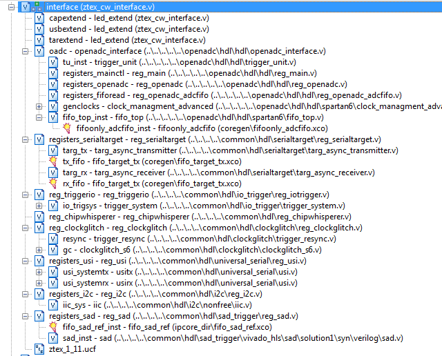
The FPGA project is fairly complex, but designed to remain as reasonably modular as possible. The hierarchical view of the source code from the ISE project navigator looks as follows:
The design is partitioned into two main clock domains, using appropriate methods for crossing clock domains (dual-port FIFOs, rdy/ack flags). The two domains are: the ADC sampling system domain, and the USB interface domain. The ADC domain is constrained to meet 100MHz, and the USB domain is constrained to meet 60MHz. Because several blocks beyond just the FIFO (such as the Sum of Absolute Difference trigger) also need to cross clock domains, and because of the extremely complex dynamic clock routing in this project, the clock domain crossing is of critical importance.
The system is designed around a simple 'base' USB communication block. This allows simple reuse of this project for work well outside of embedded hardware security. In fact the base ADC modules have already been designed as a separate project, see the OpenADC Example.
Adding a block effectively means adding it to the main bus. Each block has an address assigned, and from the Python code you can read/write to any addresses exposed by that block. Each 'address' can work in multiple ways: they can be standard byte-wise registers, OR they can be a FIFO type operation. For example when operating as a FIFO mode, it means if you wrote [0x9A, 0x8F, 0x32] into an address, this has actually loaded those three bytes into a FIFO. Similarly multiple reads from the address unload the FIFO.
This project has a number of FPGA blocks - all the ones below I've designed as part of this project, and not pulled from somewhere else. Many of them can be ripped out for use in your own project (I've tried to keep everything as modular as possible). Where possible I re-used existing blocks, such as for the I2C/UART. Here's a few of the specialized blocks that I think are particularly interesting:
Sum of Absolute Difference (SAD) Trigger
This system is capable of detecting a pattern in analog data, and triggering the capture on this pattern. This compares an incoming series of samples from the ADC to a reference waveform in real-time. I'm using this to trigger on some pattern corresponding to a specific instruction execution or program flow branch, but you could use this on any project requiring advanced ADC triggering.
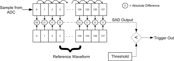
The SAD system was generated with High Level Synthesis (HLS) from C code, providing an interesting example of integrating a Xilinx Vivado HLS project into a normal ISE-style project.
Digital Pattern IO Trigger
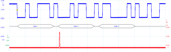
The digital pattern IO trigger detects a digital 'pattern' of 1's and 0's. There is some jitter allowed in this IO pattern, meaning you don't need precise timing on each 1/0 transition, but can put ranges which the transition must fall within. The system in the ChipWhisperer is used to trigger on a specific byte or sequence sent over a serial link such as UART or I2C. In the following the blue line is being monitored for a specific byte - you can see once that byte is transmitted the red trigger output goes high for a clock cycle.
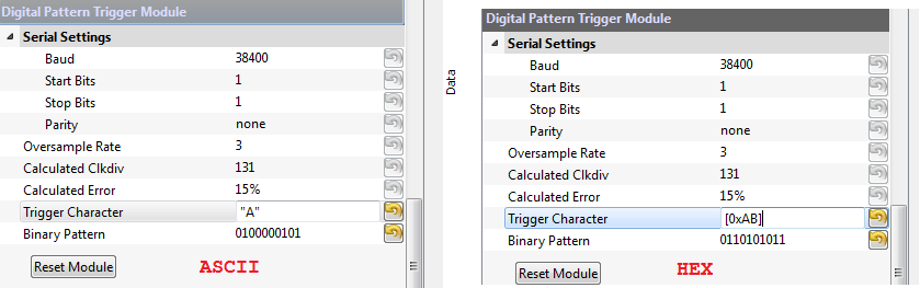
As one of the largest uses for the digital pattern IO is to trigger on a UART byte (i.e. when I send the 'encrypt' command, trigger), the GUI provides a useful screen for determining the bit pattern to trigger on. The following shows two examples of this, either triggering on an ASCII character or triggering on a hex value:
Partial Reconfiguration
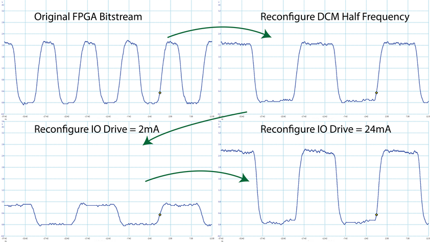
Partial Reconfiguration (PR) lets one re-write the FPGA in real time. This is used in high-end FPGAs, but there is no official support for the Spartan 6 device used here. But I required this to allow me to fine-tune the clock manager parameters from my GUI, as certain parameters in the Spartan-6 device are fixed at design time.
You can use this block like I did (fine-tuning DCM blocks), but you can change anything else that is fixed at implementation, such as changing drive strengths of the output pins as shown here, something you normally do via editing the .UCF file and regenerating a bitstream:
I published some details in a Circuit Cellar article, which has an associated online blog post. It turned out that partial reconfiguration isn't fully supported on the Spartan 6 FPGA, so this work is probably of use to a lot of other people. I also made a demo project which breaks out the partial reconfiguration block and USB interface, which is used in my half-hour video demo.
USB Interface
A huge portion of this system is USB communications from the PC. The USB block is also the master controller for the ChipWhisperer bus. The ChipWhisperer bus was designed to allow maximizing the USB bandwidth, and allows a transfer on each clock cycle. This reduces the speed the FPGA code needs to run at (i.e. you don't need to run at 2x the speed due to wait cycle requirements) while allowing the entire sample buffer to be downloaded over USB.
In addition the interface block is designed to work with a number of hardware options, and isn't tied to a specific USB interface solution. I routinely use the interface module with the following USB chips:
- Generic USB-Serial chips (CP2102, etc)
- FT2232D/H (High-Speed USB)
- Cypress EZ-USB (High-Speed USB)
From both the FPGA side and the Python API the 'middle ground' of the USB interface is completely hidden. Thus you can take the same FPGA code and move it from a platform with a high-speed USB to a platform that only has a serial port! Your transfer speed will be slower, but it's nice having that ability to move things around. This is a critical feature that makes ChipWhisperer so flexible, since you can port it to almost any FPGA board you might have around.
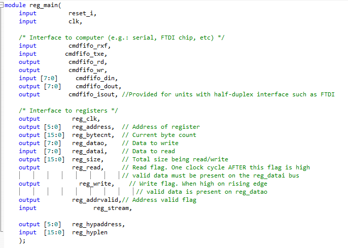
The main Verilog interface module looks like this, where a small module must interface between your physical link and the 'cmd fifo'. Examples exist in the ChipWhisperer project for serial, FTDI chips, and my EZ-USB firmware.
The Python API simply looks like this:

Where 'mode' is read or write mode, address is the address of the register (or FIFO), and the remaining parameters define data to send or maximum data to return.
Clock Routing
The ChipWhisperer has some pretty interesting clock routing, as it uses multiple muxes to select input clocks, switchs different FPGA blocks into the clock path, and routes the resulting clock to multiple possible outputs. This work can be used for your own projects that require dynamic clock adjustments. This includes drivers for both dynamic frequency and phase adjustment of the DCM blocks in the Spartan-6 FPGA:
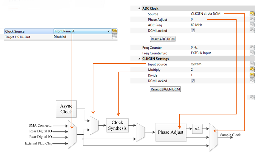
From the GUI, there is also a system to generate a specific requested frequency, in which case the system calculates the appropriate values for the Multiply & Divide settings to download to the hardware. A frequency counter on the output lets the user confirm that values are as expected, and some gross error hasn't crept in (selecting wrong input, etc).
Glitch Generator
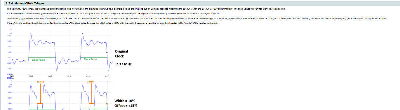
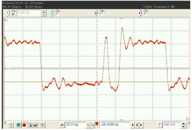
The glitch generator is responsible for generating a high-precision pulse, used for either clock glitching or power glitching. The architecture of the glitch generator built into the ChipWhisperer gives you around 100pS resolution on glitch width along with offset from the device clock edge. The end result is you have the ability to do things like repeatedly cause certain bits to be set to zero or one. Here's an example of a clock with a glitch inserted into it:
Glitches are generated by phase-shifting two references, which allow the glitch to maintain a known and constant phase relationship to the original input clock:
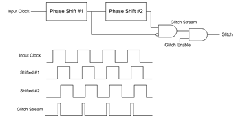
The glitch can be inserted into a clock, output on it's own, and triggered by the various systems in the ChipWhisperer. There is also adjustable glitch length in terms of cycles to glitch, and delay from trigger event.
Project File Generation
Dealing with the Xilinx ISE project file + COREGen files in a GIT repository led me to creating my own management solution. Basically it writes everything into a simple file, which gets automatically converted to the Xilinx ISE project files (which are XML based). I talk about this more in the associated project log, so go there for all the gory details.

Capture Software
The capture provides the interface to the capture hardware (be it the ChipWhisperer capture hardware or something else). The main window looks like this:
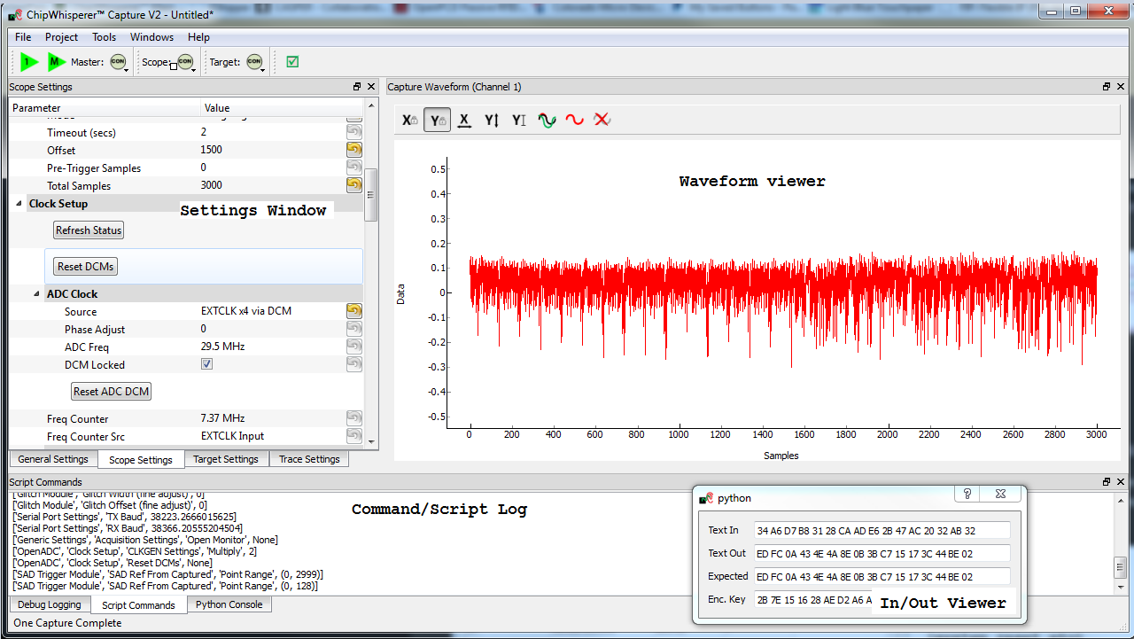
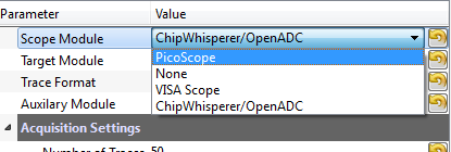
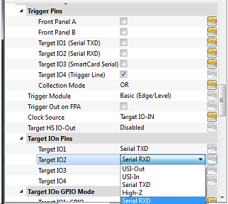
The settings window has a variety of settings, specific ones depend on the scope module selected:
These setting widgets make it easy to see what settings are available, and make changes to them:
Whenever you change a setting, a log of that is recorded in the 'command/script log' window. One can copy/paste those settings into a script file which will recreate all your settings through the GUI. This can also be used to record settings, a useful feature on complicated scope setups.
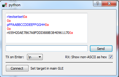
A simple terminal emulator lets one connect to a serial target device, this is useful when using the I/O blocks built into the ChipWhisperer capture hardware. Non-ASCII characters are converted to hex and displayed in red.
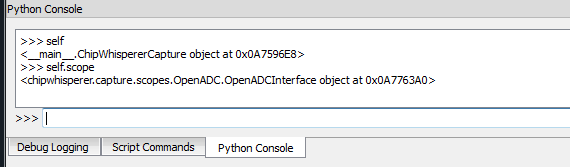
Another handy feature is the 'Python Console'. This allows you to access the python objects directly - consider for example a scope API might have features not exposed in the GUI. With the Python Console you can reach out and touch the scope module in real-time, this is useful especially when connecting to a new target where you aren't sure what data format the API is expecting for example. You can experiment on the Python console before writing the full interface module.
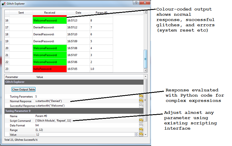
In addition there is a 'glitch explorer' window. This allows you to tell the system to automatically vary some parameter (such as glitch width, offset, delay from clock edge, etc.) and record how the system responds to a glitch attempt. This is required to fine-tune the variety of possible settings in the glitch system.
Analyzer Software
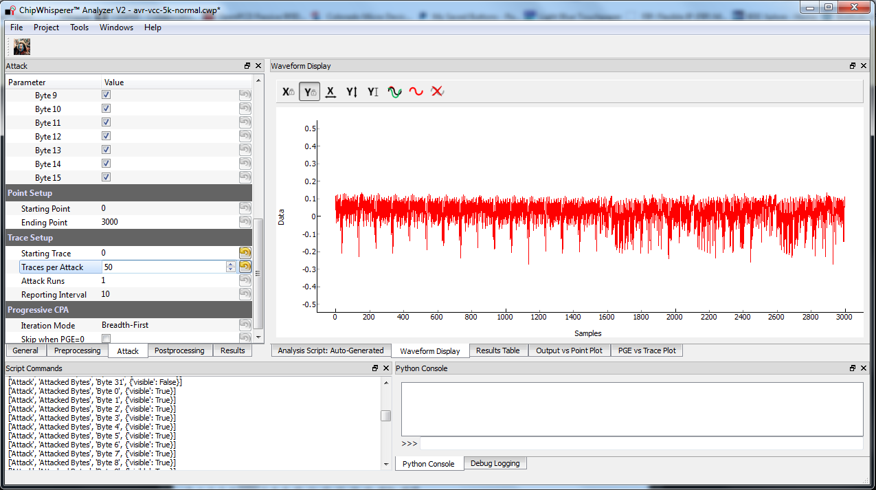
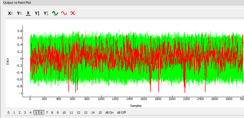
When running an attack, the output can be graphed against sample point. In the following example we can see the exact point in time where byte 5 & 6 are being attacked:
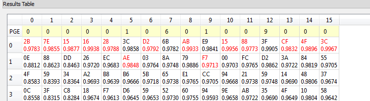
The result table can sort attack guesses by correlation value (or other attack).
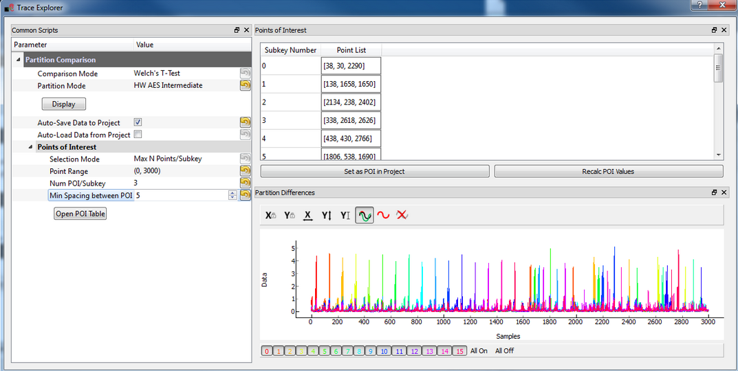
Another feature is what I call the 'trace explorer'. This allows you to take a trace, and determine if a leakage is appearing at some point.
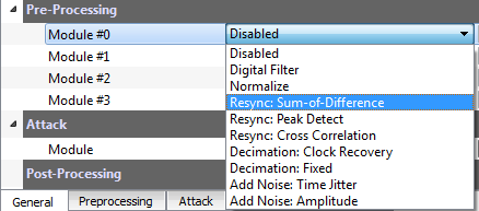
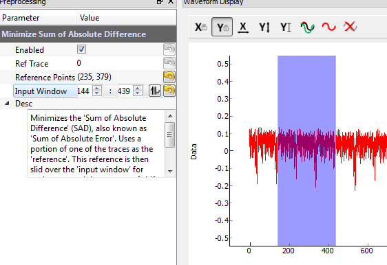
When using the analysis software, the preprocessing modules can be chained together with the GUI. For example let's enable the 'Sum of Absolute Difference' synchronization:
We can then select the points of interest from the graph widget:
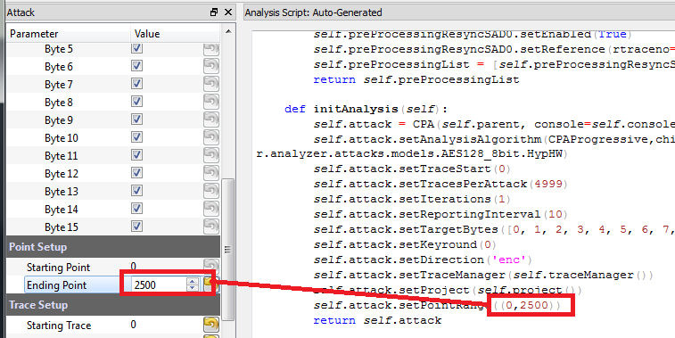
When setting parameters from a GUI, they are written into a standard Python file. This Python file is the 'analysis script'. One can copy/paste the analysis script to create a full-featured attack, for example by adding your own custom modules that aren't configured via the GUI. The seamless interaction of the GUI and analysis script file gives you the best of both words: it's easy to make quick changes via the GUI, but you aren't constrained to modifying things through the GUI only. You can import Python modules, add your own logic, or anything else to the analysis script.
Plotting and Graphing
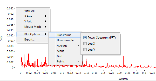
The plotting module is based on PyQtGraph, which provides many useful features, such as the ability to switch between a FFT and time-domain view. This can be useful during investigation of the leakage to determine if leakage involves certain frequency bands for example, or the context menu can be used for exporting data in various formats (PNG, CVS, etc):
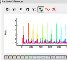
A number of improvements are built into the 'GraphWidget' class, which when combined with the various display modules (such as the PartitionDisplay module) add features such as the toolbar for zooming/locking axis, persistence display of multiple traces, highlighting certain bytes with different colours, and displaying minimum/maximum over a huge number of traces. This screenshot (part of an earlier screenshot) shows some of these features:

The ChipWhisperer analysis software supports database storage for traces. This can be done with a MySQL database, although it's fairly easy to add support for other formats. Because most of the traces are fairly small I haven't bothered to investigate use of databases designed for huge amounts of data, but if you wanted to use millions or more traces, you might start to investigate other options. When using database support you could make a simple diagram like this:
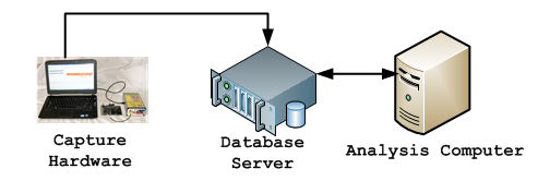
Which at first might seem dumb - why is that better than storing to a file on disk? There's a few reasons that even when working in a local lab you might want a database connection instead of a file:
- Allows analysis and capture to occur simultaneously
- Capture lab is physically separated from analysis location - capture over the weekend in the lab, but am working from a laptop remotely, and always have access to the latest data via network connection
- Capturing from multiple physical devices instead of a single target
But the biggest push for the database support is so you can use cloud computing! Analysing a large number of traces or when dealing with more advanced attacks could take a long time on a standard computer. Analysis times from hours to weeks aren't unreasonable, and the amount of time it takes is always part of the 'how secure is this system' question.
The analysis is frequently an embarrassingly parallel problem. As a simple example you can split each of the attack subkeys into a separate process with no changes to the software. Similarly you can split the traces into multiple point ranges to sub-divide the task further. This assumes you have lots of computers to work with - if you are just a gal sitting at home with a cheap laptop this might not be the case. Luckily all you need is a credit card to solve this - Amazon lets you rent access to both a database service along with cloud computing. This means you can save all your storage data to a database server, and then run the analysis on a rented high-performance cluster, which has high-speed access to your saved traces. This would look something like this:
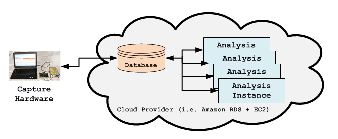
The ChipWhisperer uses connectivity to eliminate the old assumptions that an attacker without the resources to build a computer cluster can only achieve some limited success rate. Support for remote connectivity allows an attacker to rent the resources, at what are realistically very minimal charges (i.e. $504 could get you 24 hours of access to 50 computers, each one with 8 CPU cores, 15GB RAM, and 160GB of SSD storage). Amazon EC2 makes it easy to target different algorithm types too - you can request individual nodes with up to 244GB of RAM with the click of a button.
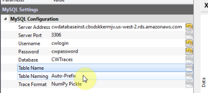
The MySQL configuration can be done from within the ChipWhisperer software, as one of the 'trace writer' modules supports the MySQL database format. If you want more details be sure to see the full example of connecting to Amazon database service. Here's a shot of the MySQL connection:
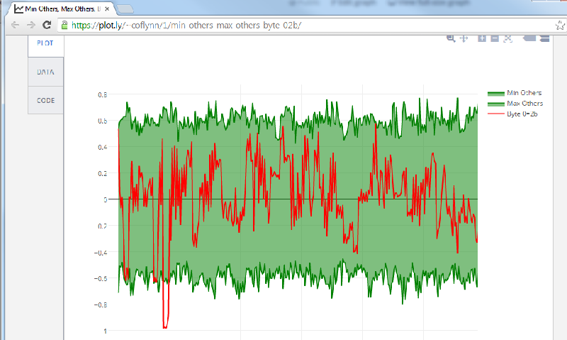
The results can then be pushed directly to plot.ly to make data collection easier (see log post for details):

The software itself can connect to a variety of hardware devices, not just the ChipWhisperer hardware. Here is an example where we are performing power measurements with a PicoScope with a homemade target board. There's a video demo of using a PicoScope to attack a FPGA-based AES implementation too, see the list of videos.

If you do want to use custom hardware, you can use a variety of FPGA boards, not just the special hardware I've designed. A large list of these is shown in the wiki, but this section shows a few of the options I've tested. The lowest cost option uses an Avnet LX9 FPGA ($89) board with the OpenADC module, as shown below:
This device doesn't have all the features of the complete Spartan 6 LX25-based capture hardware, but it is considerably cheaper! The smaller Spartan 6 LX9 means the advanced features such as the SAD trigger cannot fit into the FPGA design, but the basic functionality remains.
Two additional boards are of interest to the research community - the SASEBO-W which is used for smart-card based research. The OpenADC board can be plugged onto this board, and a version of the FPGA bitstream programmed into the huge Spartan 6 LX75:
The other board is the SAKURA-G, which has both a Spartan 6 LX9 and LX75 FPGA. This board is useful for attacking FPGA-based implementations. Again the OpenADC module can be mounted on this FPGA board:


H-Field Probe
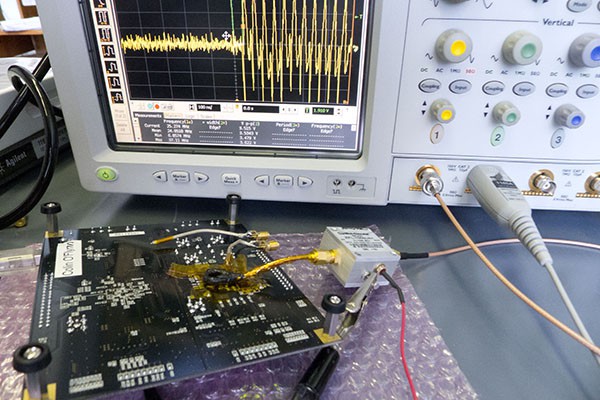
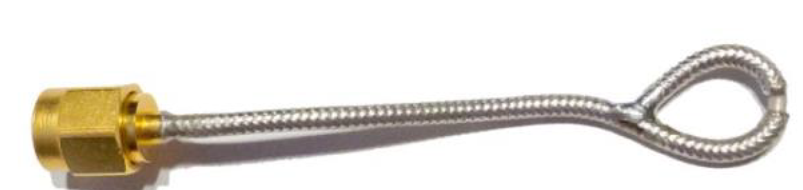
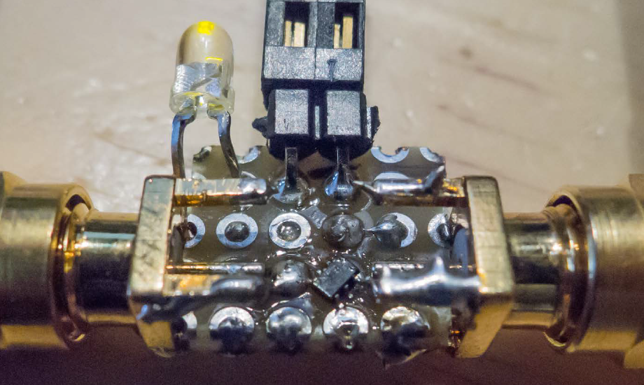
Rather than inserting a shunt into a circuit, it's also possible to use an H-Field (magnetic field) probe. This allows us to monitor the current with a simple probe placed onto the circuit, possibly even from outside the casing itself. You can purchase such probes, but they tend to be pretty expensive ($500-$2000). Here's an example of me probing a FPGA using a magnetic field probe I built, along with a commercial Low Noise Amplifier (LNA) for connection to a regular oscilloscope:
So instead I've added some instructions for making your own from a length of semi-rigid coax, which you can buy from ebay for a few dollars, or from Digikey for about $10.
Low Noise Amplifier
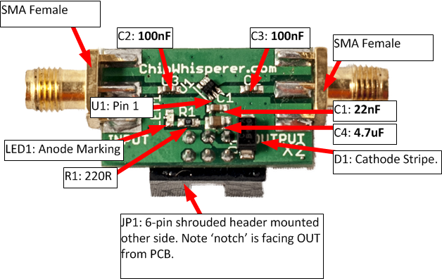
When using a H-Field probe, one often needs a low noise amplifier. Commercial LNA designs can be at least $100 - which is silly when they can so simply be built. I made one around a small chip, which can even be built with protoboard, which looks something like this:
But if you build one with a nice PCB it looks something like this, where part values have also been noted (see links from hardware section for BOM/PCBs):
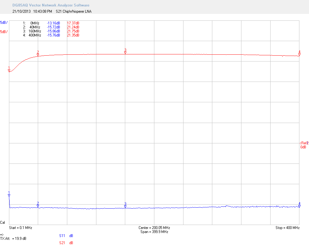
Which for as implemented has the following gain & input match parameters (S21/S11):
Differential Probe
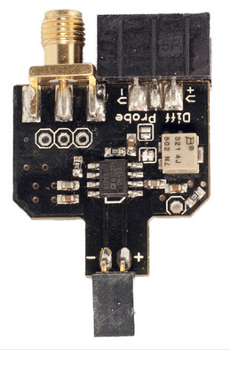
Another useful piece of equipment is a differential probe - which again can be very expensive ($1000+). We can use about $25 worth of parts to build our own, which works 'well enough' for most differential power analysis attacks (see links from hardware section for BOM/PCBs):

One of the core underlying theories of this entire project is that the measurement of power is synchronized to the device clock. This differs from normal oscilloscopes, as they run with an internal timebase. Some scopes will permit you to use an external timebase, but often with a number of caveats, and without providing the clock modification functions (integer multiply/divide, phase shifts).
The ChipWhisperer system by comparison is designed to interface to a target device, and use the target device clock to maintain perfect synchronization. The target device clock can be multiplied, divided, or phase shifted as required. You can read some details of this in a paper on the ADC system, along with the paper on the ChipWhisperer, two of my peer-reviewed conference papers on the use of synchronous sampling.
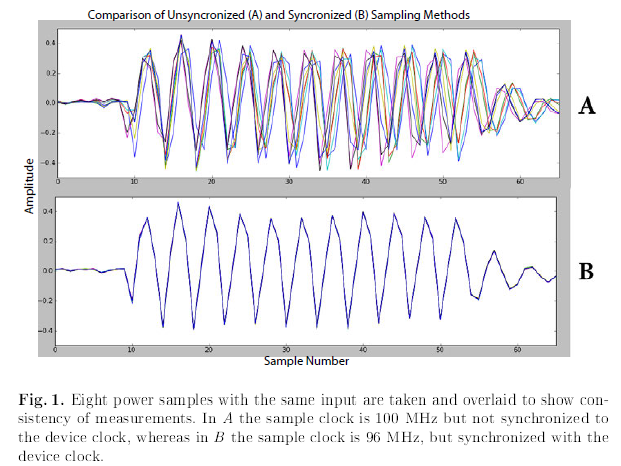
The synchronous sampling ability is actually a core feature of the ChipWhisperer, as it allows you to perform attacks at considerably lower sampling rates. Attacks that were reported to require a 2GS/s oscilloscope can be accomplished with a low-cost ADC when synchronous sampling is used. The following shows a comparison of asynchronous and synchronous sampling, where eight overlapping traces when measured with synchronous sampling show almost zero jitter (in B):
As an interesting additional feature, you can perform clock recovery on a device running on an internal oscillator. The system to perform this looks something like the following block diagram:
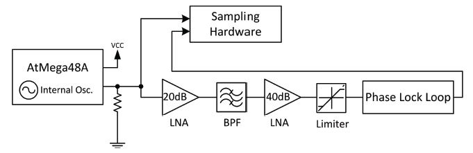
Which allows us to detect the fundamental frequency, and then use that frequency for digitizing. If you are interested in this see my journal paper on this topic. The clock recovery hardware is part of the ChipWhisperer project, and for example you can find a BOM here.

Component List
There is a huge number of options when you want to build this - I've listed some basic components on the hackaday.io project here, but for the full list head over to the wiki page. This includes even things like a copy-paste list you can order from Digikey for the main PCB, easy!
PCB Gerber Files
Links to all the gerber files were given in the 'hardware' section.
Assembly Instructions
Links to details of assembling each board are given in the 'hardware' section. Details of building the complete system are included in the wiki, and a few examples are included on this hackaday.io page.

Here's some videos that cover different aspects of the project:
Instructional Videos
ChipWhisperer Software: Driver Installation on Windows 7
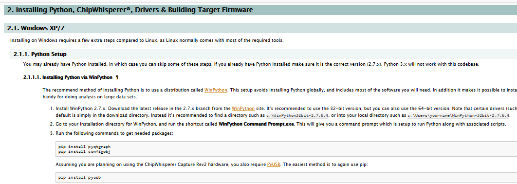
ChipWhisperer Software: Python Installation on Windows 7
ChipWhisperer Software: Building AVR Example Target
ChipWhisperer Tutorial: Glitch Attacks
ChipWhisperer Tutorial: SAD Trigger
2.5 Hour Tutorial on Side Channel Analysis
ChipWhisperer + MySQL Demonstration using Amazon Web Services (AWS)
ChipWhisperer Glitching Example: VCC Glitching Android Smartphone
ChipWhisperer Glitching Example: VCC Glitching Raspberry Pi running Linux
ChipWhisperer Glitching Example: Clock Glitching AVR Microcontroller
Hardware Security: Timing Attacks on PIN-Protected Hard Drive
ChipWhisperer with SAKURA-G (FPGA-based AES) using USB-Based Oscilloscope