Alain d'Espaignet
Images cannot be in the project section so here is a recap so you get the idea:
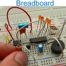
Suppose I give you a battery a resistor and an LED.
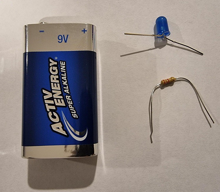
Can you not simply by holding the parts in your hand make the LED light up?
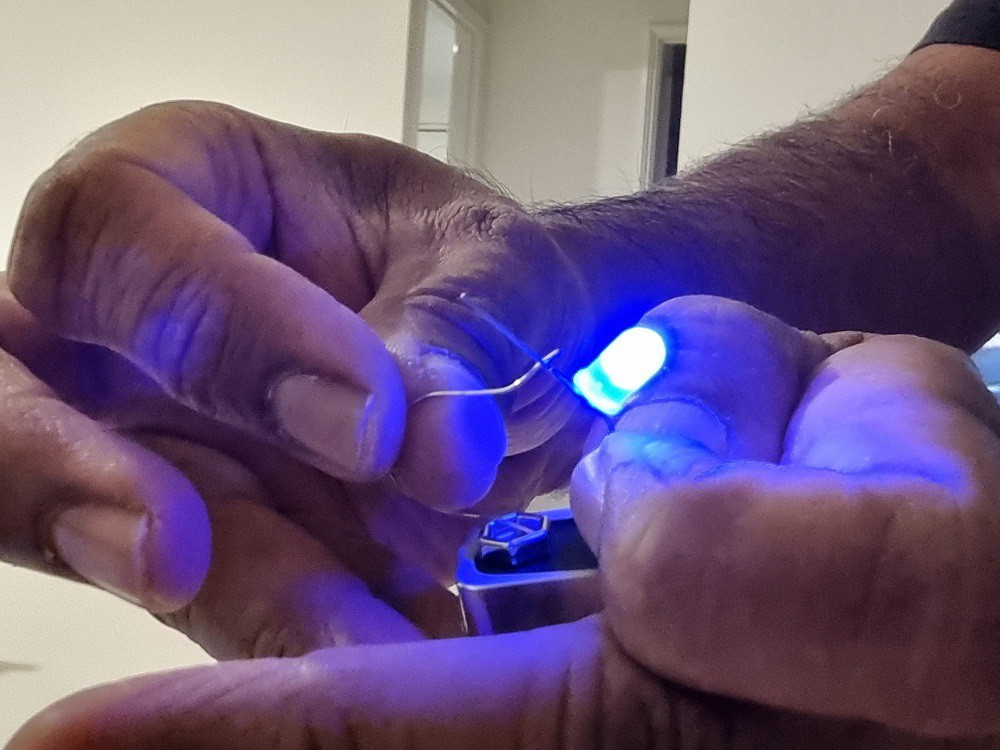
All you need is for things to make contact so electrons flow and it will work.
PS: The country where I live is remote and shipping costs a lot plus it is a small market. I ordered an LED from a local online store. It took 2 weeks to fill the order of 1 LED and 1 resistor and that after I had to call to remind them they had a pending order. The one LED I purchased for Rs 2 did not work! Can you believe it! Bad luck. (: Fortunately my friend from New Zealand bailed me out with the pictures I wanted to show to illustrate the concept above. Thanks Collin.
Have I convinced you yet? Now read on...
Unless you’ve been living under a rock or in a cave in a remote place with no modern form of communications you should be well aware that we have a problem with electronic waste all around the globe.
Just search for e-waste on Youtube or Google and you’ll find grim titles such as:
How e-waste is harming our world
E-waste: Why We Need to Act Now
The explosive problem with recycling old electronics
E-waste: How big of a problem is electronic waste?
…
I stop at a few but the list goes on and on.
The thing that surprised me watching some videos about the recycling process is that inevitably the first step after some disassembly and the removal of batteries is the grinder!

Everything goes through the grinder and comes out as a fine powder. Then the material recovery process begins.
Nothing is reused as is really.
Gee is that the best we can do? Really?
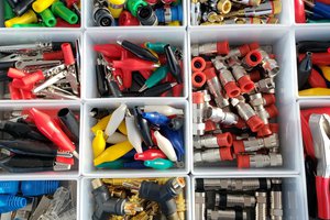
Imagine the millions if not billions of electronic components that are most likely good to be reused as is that we grind up!
What if we could recover and reuse most of those!
Ahh but it costs too much to desolder to recover them you are thinking.
Just crush it all up and we'll see what metals, plastics and fiber we can recover from that.
That’s good enough. Who cares anyway. That's a messy business with a small margin anyway.
What if I told you we can do better!
How is that ? Said by the naysayers.
I hear you. Every new idea is often met with resistance and ridicule in the beginning.
In putting up my idea for this competition I might be subject to a lot of criticism but I am taking that risk.
Some may think I have fallen off my rocker!
I ran the idea through a few veteran electronics freaks I know and they thought:
That’s thinking out of the box - Collin Pillay.
That could be useful, do put the idea out there - Deon Smit.
I’ll spare you the morality speech as to why we should at least try to reuse and recycle at some level and introduce you to my lunatic idea.
Fundamentally it goes like this:
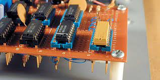
Suppose we did not solder electronic components on printed circuit boards at all.
Imagine how many good things could come of this.
For starters we can easily get to the components to repair, recover and reuse.


 Brien Allison
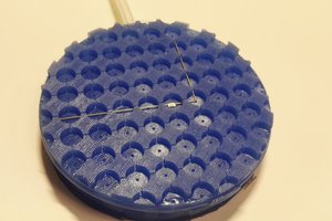
 Inne
Inne
 Giovanni