 Keith
KeithMicro Cornucopia number 32, (October/November 1986)
Public Domain 32000
By Dave Rand and George Scolaro
72 Longfellow St. Thousand Oaks CA 91360 (805) 493-1987
World’s Cheapest Unix System
Contents
- Public Domain 32000: The Hardware
How to put together a UNIX co-processor system
(complete with UNIX V) for under $1,000. - Public Domain 32000: The Software
The software end of this UNIX compatible. - PALs — What They Are And When To Use Them
Why the 32000 UNIX system was designed with PALs
The Hardware
This is for all of you who want to put a computer in your clone or CP/M machine. (Sorry, that was a cheap shot.) Actually, this is the cheapest way known to hacker or human to build a truly powerful system (UNIX System V if you wish).
With hardware floating point that outruns DEC 11-70s, 2 Meg of DRAM, DMA, and a memory management chip, this $400 system is an incredible hardware bargain. See the SOG V article in this issue for information on a public domain operating system for this machine.
Our primary goal in designing 32000 based system was to come up with a low cost system without compromising performance. One of the unique aspects of the design (which was first presented at SOG V) is that it has been released to the public; schematics, PAL equations, interface software, and the PCB artwork. For this reason, we named our design PD32. (We are, however, restricting commercial copying of the system, see the note at the end.)
We chose the National Semiconductor 32000 chip set (second-sourced by Texas Instruments) because it’s inexpensive, is a mature product, and was designed to support high level languages. The total cost of both the hardware and UNIX System V, with which the system runs, should be under $1000.
The version of UNIX available for this board is the full AT&T UNIX System V release 2. The port was performed by ZAIAZ Communications and is AT&T and National Semiconductor approved.
About The 32000
The 32000 series includes the timing control unit (TCU), the central processing unit (CPU), the memory management unit (MMU), the floating point unit (FPU), and the interrupt control unit (ICU). Currently four CPUs are available in the 32000 series; they are the 32008, 32016, 32032, and 32332.
The 32000 series is unique in the microprocessor world in that it is the only family that maintains 100 percent upward and downward software compatibility at the binary level. This compatibility means the end user doesn’t need to change software when changing CPUs.
Of the four CPUs, we chose the 32016 for its price and ease of board routing (the board has only two layers). The 32016 still has a full 32-bit internal architecture but has a 16-bit external data path. To reduce pin count both the CPU and MMU multiplex their data and address buses. In other words, data and address information are put on the same set of pins.
Hardware Design
Now that we’ve covered some of the background, let’s take a close look at the design. From Figure 1 we can see that the TCU, CPU, MMU, and FPU figuratively bolt together. To understand how the rest of the system interfaces to these four devices, we need to understand the timing of a bus cycle.
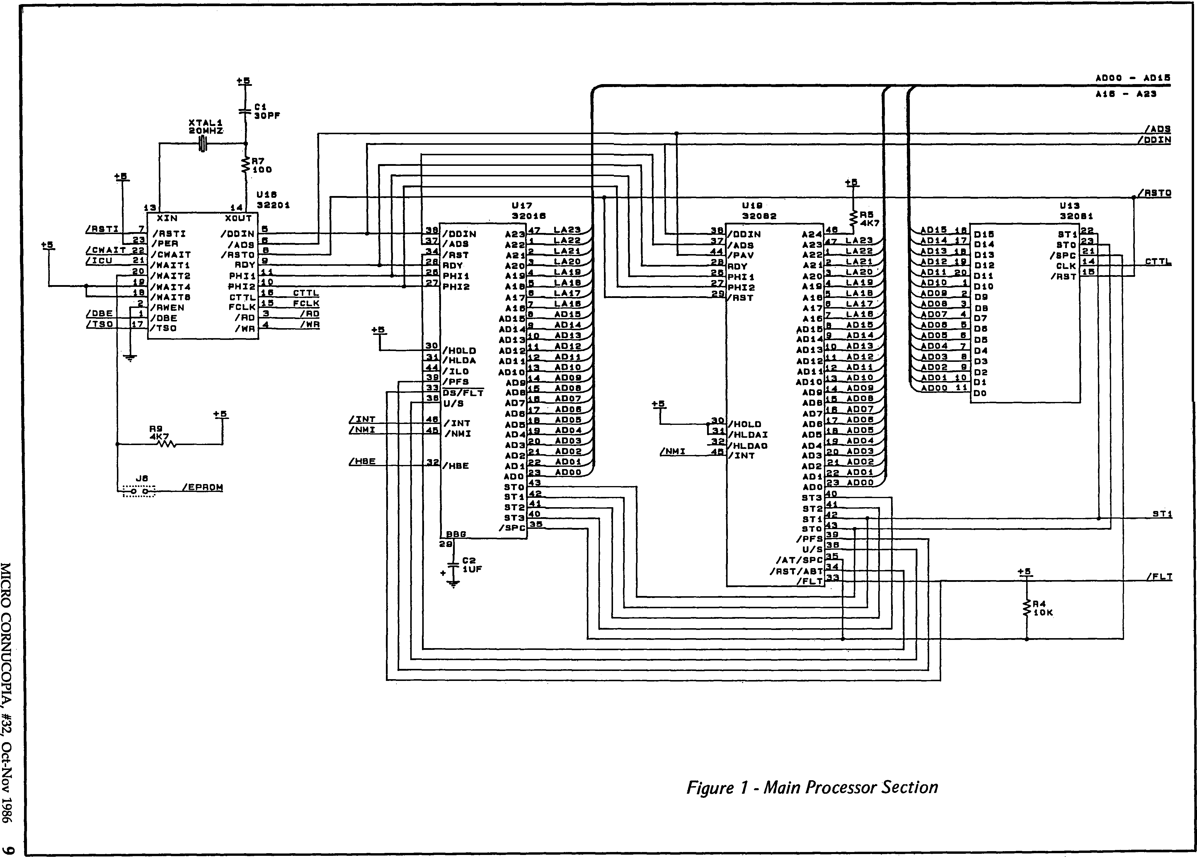
Figure 1. Main Processor Section
Addressing
The CPU places the logical address onto the data/address bus during T1 and pulses its address strobe (ADS) pin. If an MMU is in the system (as in this design) ADS from the CPU connects to ADS of the MMU. The MMU then performs any necessary page table lookups and translations, places the physical address onto the data/address bus, and pulses the physical address valid (PAV) pin. This is performed in the TMMU state.
This pin becomes the system-wide address strobe pin and also connects into the TCU. The TCU, on receiving the ADS signal, generates either a read (RD) or write (WR) signal during T2 and T3. During T2 and T3 the bus becomes a data bus with data either being read or written by the CPU or MMU. The final T4 state is used internally by the CPU to prepare for entering an idle bus condition (if the 8-byte prefetch queue is full) or for starting a new T1 state.
Wait States
Since the TCU generates the RD and WR signals, wait states may be requested by asserting either the CWAIT, PER, or WAITn signals. The TCU. generates READY, which the CPU and MMU sample and wait on as necessary. The CWAIT is a continuous wait signal. WAIT1, WAIT2, WAIT4, WAIT8... allow from 1 to 15 wait states to be digitally selected. We did not use the PER signal in this design. It modifies the bus cycle so the 32000 can talk to slow peripherals such as UARTs.
The TCU generates several other useful signals: data bus enable (DBE) which is used to enable data bus transceivers (which don’t exist in this design), timing state output (TSO) which is a signal that comes out very early in T2 and lasts through T3 (used by the DRAM controller), CTTL (TTL buffered PHI1), and FCLK (crystal frequency).
Latching And Decoding
Since the data and address buses are multiplexed together we need to separate them into two buses for the EPROMS, the ICU, and address decoder PAL (U3 DEC32). Figure 2 shows U14 and U15 which latch the 16 least significant address lines using the inverted system address strobe signal (ADS). The high order address lines A16 to A23 are latched by the CPU/MMU for the full bus cycle, so at this point we have a separate 16-bit wide data bus and 24-bit wide address bus. The DEC32 PAL takes several of the address lines and generates the PPORT, INT86, EPROM, ICU, and RAMS signals. PPORT is the select for the parallel port which forms the PD32-to-host data interface. INT86 is a signal used to interrupt the host or set a flag that the host can sample to see if the PD32 has a request waiting for service. EPROM is the select line for the two EPROMS (remember the 32016 has a 16-bit wide data bus). ICU is the chip select for the ICU, and RAMS is the chip select for the dynamic memory.
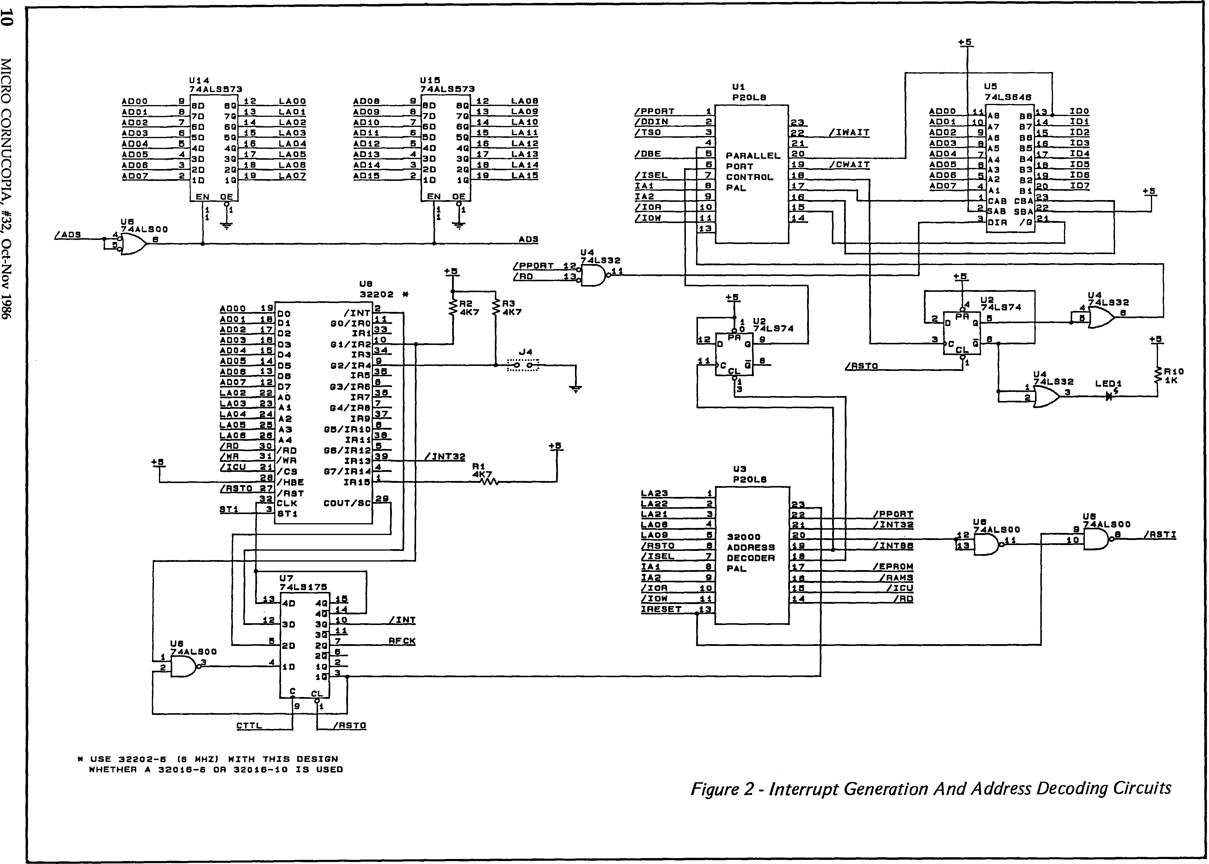
Figure 2. Interrupt Generation And Address Decoding Circuits
DEC32 also generates a software reset signal that is combined with TRESET (the power-on reset signal from the host) which connects to the input reset pin of the TCU. DEC32 also takes several of the host signals (ISEL, IA1, IA2, IOR, and IOW) and generates a signal to clear the flip flop U2 (via pin 13). This half of the flip flop is set whenever the PD32 attempts to interrupt the host. Thus the host may honor the interrupt (the Z80 host design does not use interrupts), or it can poll the interrupt status via a status read.
Parallel control PAL U1 takes the output of the interrupt status flip flop and makes it available on IDO. U1 also generates the signals to clock data into the data latch when either the PD32 or the host performs a data write cycle, and the data enable output signal when either the PD32 or host performs a data read cycle.
The data latch is a 74AS646, a very handy chip. It has two back-to-back transparent latches (in a glass case) with tristate capability. Thus it acts somewhat like a one-byte FIFO.
The other half of U2 is used to keep track of whether the data latch, U5, is full or empty. The PAL U1 and the flip flop form the control circuit for managing the data latch, U5. This design forces wait states on both the PD32 and the host to synchronize data transactions. Wait states are asserted if either the PD32 or host attempts to write to the data latch if it is already full, or if either attempts to read the data latch if it is empty.
We designed the software protocol so that in all situations the PD32 rather than the host will be placed in wait states. Plus, we designed the PD32 so that the DRAM continues to be refreshed even if the CPU is forced to indefinitely wait (this cannot be assumed of the host and certainly not the IBM PC/AT).
Parallel Port Vs. Dual Port
In case you’re wondering why we chose a parallel port interface rather than a dual port approach, the parallel port approach has many advantages in this design, some of which are listed below:
- very simple interface requirements on the host. The IBM PC/AT or Z80 or Slicer make ideal hosts for the PD32.
- very fast data transfer rate. 250 Kbytes/sec on a 4 MHz Z80, and up to 500 Kbytes/second on an IBM AT or PC with a V20 or V30.
- easy to debug the interface via the host by output commands with a debugger while monitoring the signals on the PD32.
- data from the host is read by a software loop on the PD32: This means that the CPU can read the data and transfer it to the logical address with the MMU actually mapping the address to the physical address. Thus, data from the host does not have to be
The last point is very important since UNIX requires that the data be transferred to the logical address. In a dual port system the host would move the data directly to the physical address. Since the UNIX System V on the PD32 supports demand paged virtual memory, logical pages are not necessarily stored contiguously in physical memory. This complicates the software in a dual port system since the host would have to read the MMU translation table entries for every 512-byte block of data it was transferring.
The ICU’s Function
The ICU performs several tasks in this design. First, it generates both real time interrupts (60Hz time slicing for UNIX) and software interrupts inside UNIX, and also accepts interrupts from the host on IR13. Second, since in this design the ICU is programmed to have eight general purpose outputs, G0/IR0 to G7/IR14, we use these to perform the following:
- When the G1/IR2 output goes low, U7’s /1Q output latches low causing the DEC32 PAL to switch out the EPROMs in low memory and select the DRAM. (On reset, the 32000 starts execution at memory location 0.
Thus we want the EPROMs at 0 initially, but once the PD32 is up and running, we want RAM at location 0.)
- G2/IR4 if low causes the EPROM software to perform a full memory test every time the host resets the PD32. This helps you debug the memory circuit.
- G3/IR6 may be monitored with a meter, and if low indicates that the self-test performed by the EPROM has failed. This information is also output to the data latch so that the host can check the status of the PD32 after the reset command.
The DRAM and EPROM are fairly self-explanatory (Figure 4). Both EPROMs are selected whether the CPU performs a byte or word access since the EPROM can be read only.
The DRAM, on the other hand, is organized as four banks of 512K bytes each. (A total of 2 megabytes is supported and automatically sized by the EPROM software.) There are upper and lower bytes (to create the 16-bit word).
The 32000 series has no alignment restrictions on data read/writes or instruction fetches. Thus the memory has to be organized so reads and, more importantly, writes to individual bytes are supported. The 32016 signals the data bus width (whether the read or write is 8 or 16 bits) using the A0 and HBE signals. If A0 is low, the low byte is active (assuming HBE is high).
If HBE is low then the high byte is active. These signals are shown on the DRAM controller schematic (Figure 3).
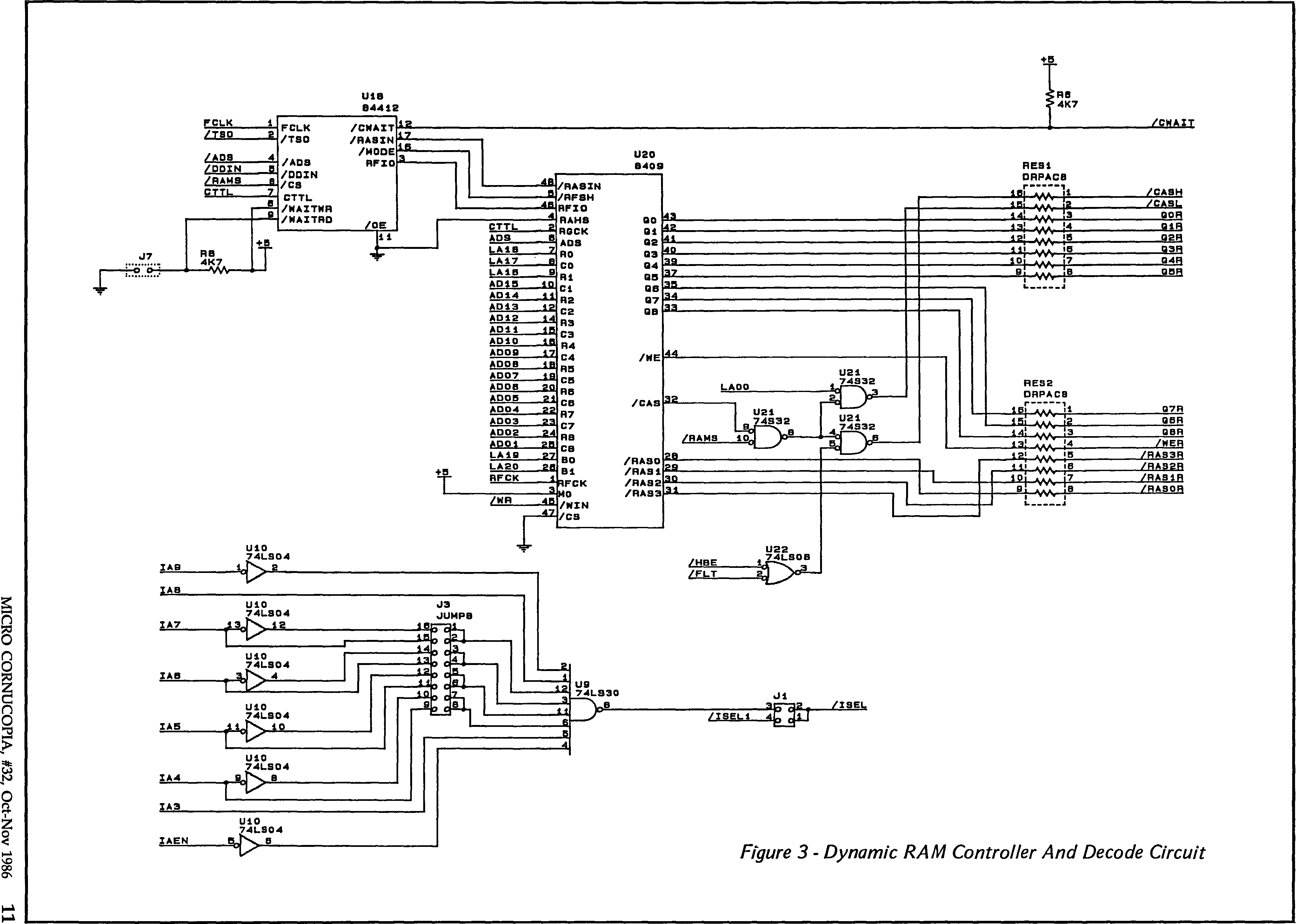
Figure 3. Dynamic RAM Controller And Decode Circuit
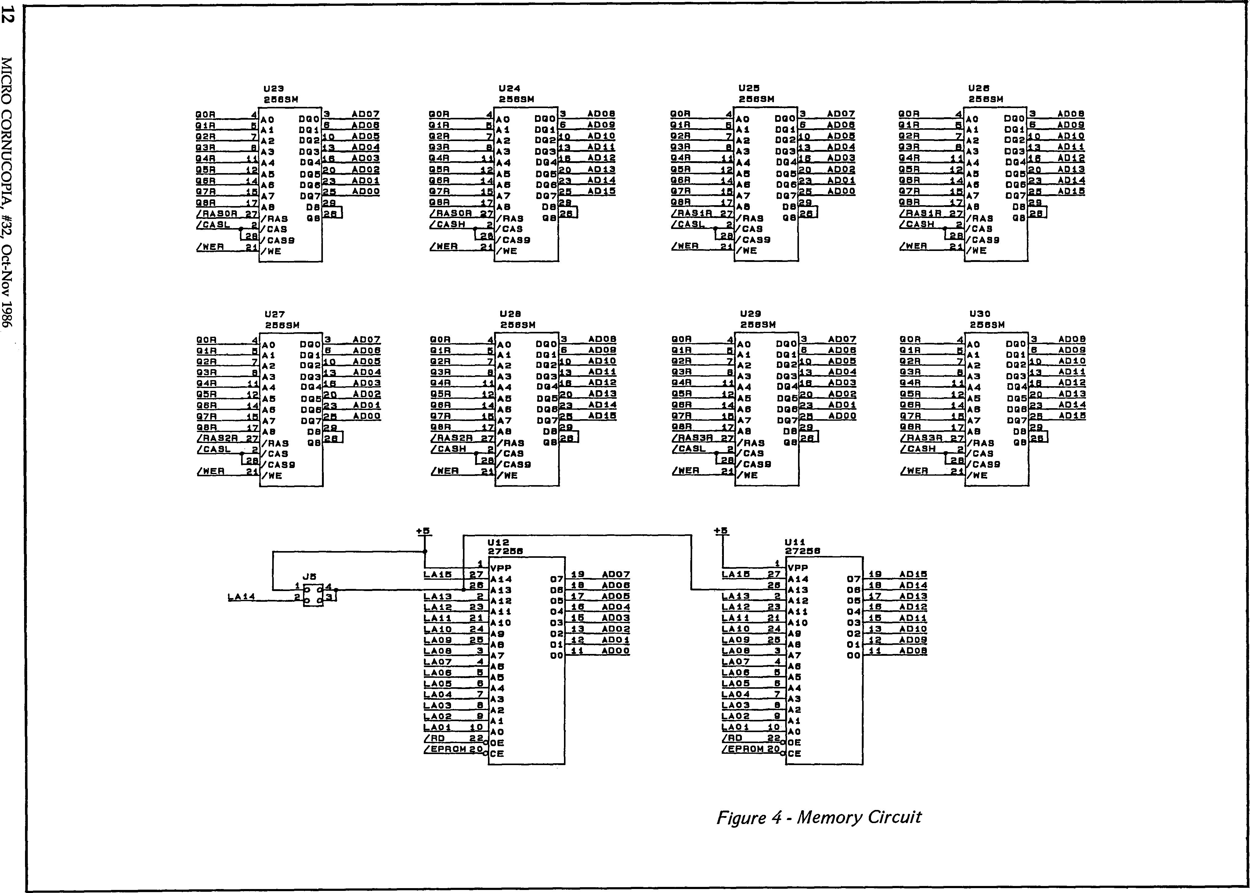
Figure 4. Memory Circuit
DRAM Control
Explaining the interaction between the DP84412 (U18) and the DP8409AN-2 (U20) is beyond the scope of this article, so we’ll just treat them as a single unit (refer to the series 32000 hardware databook). This design allows a wait state to be inserted into a DRAM read cycle by jumpering J7. Even using 150ns DRAM, you need this wait state if you’re using a 10MHz PD32 and a DP8409AN-2 (slow version). If you have a DP8419 (fast part) in the system you won’t need the wait.
U20 multiplexes address lines for the DRAMs and generates the RAS, CAS, and WE signals. All the outputs of U20 that connect to the DRAMs are designed to drive high capacitance loads (typical of large DRAM arrays).
The series resistors reduce undershoot voltages caused by fast signals from U20, PCB trace inductance, and DRAM capacitive input loads. U20 and U18 also generate refresh cycles for the DRAMs with period RFCK (16 µsec square wave from one of the internal 16-bit counters in the ICU).
The refresh cycles and CPU/MMU cycles are arbitrated by U18. Once a refresh cycle is started, U18 keeps asserting wait states until it is complete. The circuitry that generates the CASL and CASH signals for the DRAMs is necessary, first to support the byte read/write capability of the CPU, and second, the word read/write requests from the MMU when it’s performing translation table updates or fetches.
The FLT signal from the MMU causes the CPU to release the bus. In this design FLT is used as the equivalent to HBE from the CPU. The MMU will always assert A0 low since it accesses word aligned data only. One final point regarding chip select: for the DP8409AN-2 (U20). In order to use the slow (cheap) DP8409AN-2 in systems with fast clocks (such as the 10MHz PD32) and still not violate its specifications, we keep it enabled. Because it’s always enabled it will constantly generate RAS/CAS cycles for all CPU bus cycles (including accesses to EPROM, etc.). Then we use the RAMS signal to gate off the CAS signal from U20 unless we’re really accessing DRAM. Thus the DRAMs will see only a RAS cycle (a refresh cycle) when DRAM is not selected. The final part of the schematic is the decode circuitry in Figure 3 which is used to qualify the address from the IBM PC/AT. If a Z80 is being used as the host, this decode circuitry is by passed via J1, with the decoding being accomplished on a daughter board.
CONN2 in Figure 5 is used to connect to a daughter board via a 26-line ribbon cable. The schematic of the Z80 daughter board in Figure 6 shows how to interface a non-IBM PC/AT host to the PD32.
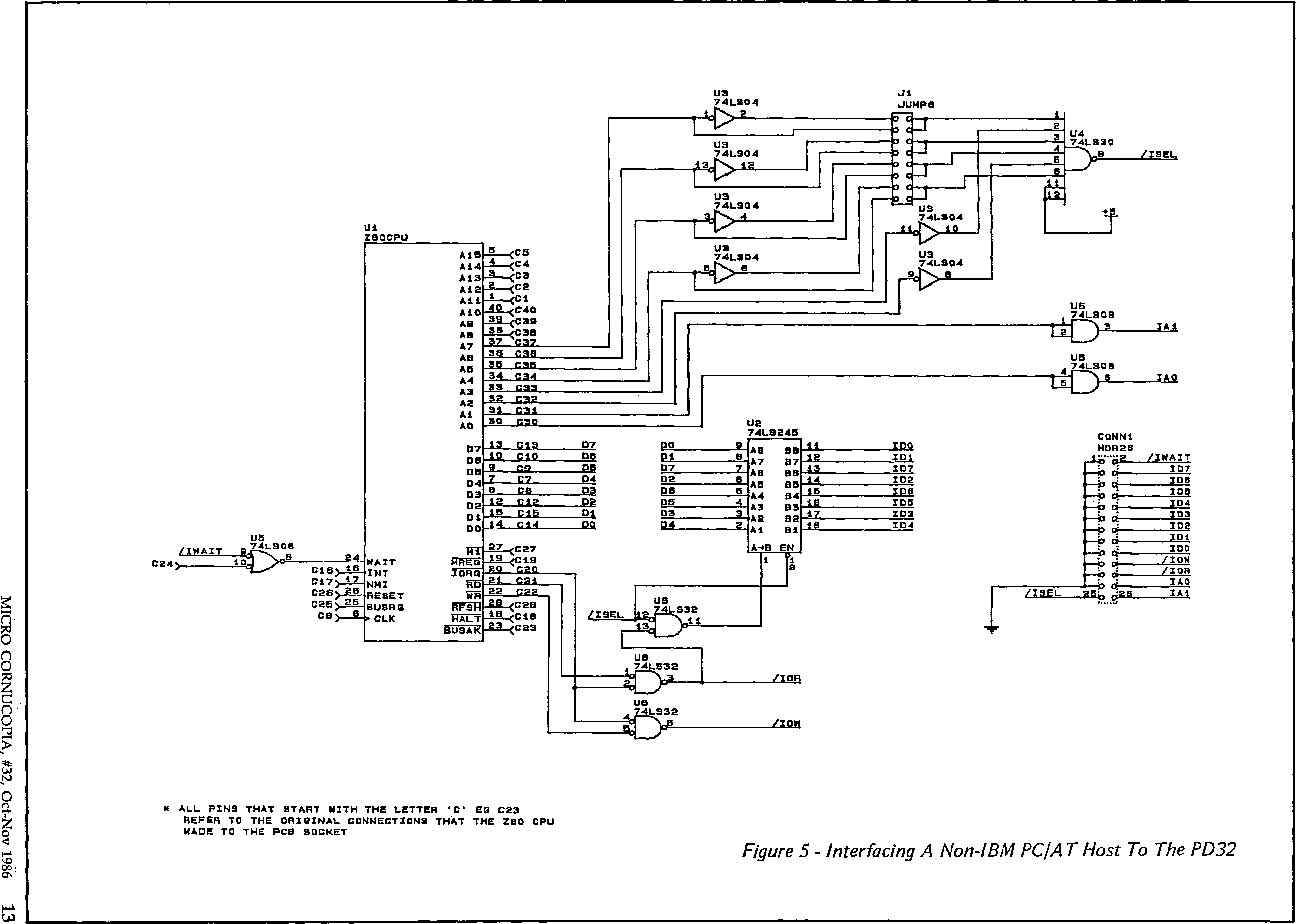
Figure 5. Interfacing A Non-IBM PC/AT Host To The PD32
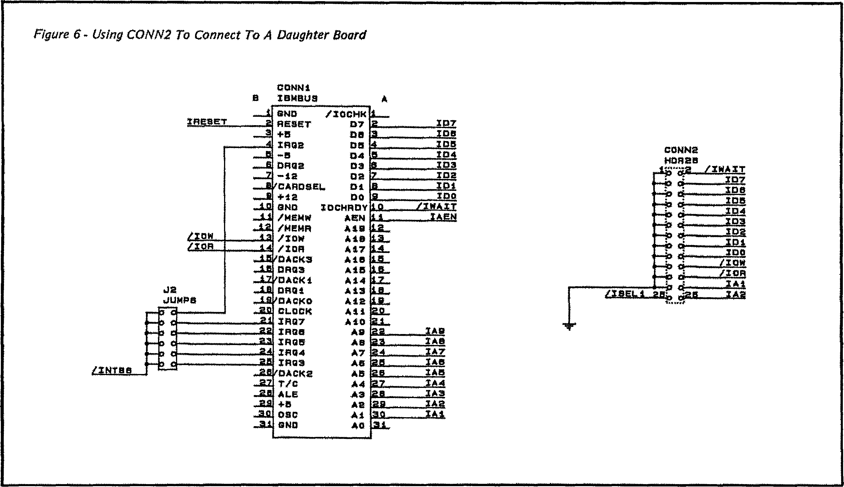
Figure 6. Using CONN2 To Connect To A Daughter Board
For more information regarding construction, debugging, software sources, and latest schematics, as well as the PD32 user’s group, contact:
Dan Efron 8910 Westmoreland Lane Minneapolis MN 55426 (503) 382-7643 (Micro C RBBS)
Note: George Scolaro is maintaining the copyright on the hardware design and is restricting copying to small-quantity, non-commercial users. Any commercial production of this system must be by license through George.
Components
U1    PAL20L8        Parallel port control
U2    74LS74
U3    PAL20L8        Address decoder
U4    74LS32
U5    74LS646
U6    74ALS00
U7    74LS175
U8    NS32202
U9    74LS30
U10    74LS04
U11    27256        D8-15
U12    27256        D0-7
U13    NS32081
U14,15    74LS573        Address latches
U16    NS32201
U17    NS32016
U18    DP84412        DRAM controller
U19    NS32082
U20    DP8409        DRAM address multiplexer
U21    74S32
U22    74LS08
U23-30    256SM        256K * 8 bit DRAM modules for 2 megabyte total

R1,2,3, 5,6,8,9    4k7
R4     10k
R7     100R
R10    1k

RES1,2    DIP16 series resistors, looks like 74.3 ohms

C1    30p
C2    1µ

XTAL1    20 MHz
Public Domain 32000: The Software
There are two tricks to integrating two systems: hardware and software. Interestingly, the best trick is the software. This is the software part of the PD32 series.
One of our challenges in designing the PD32 software was to support UNIX™ and still make it portable enough to be moved to a number of different operating environments. Thus, the software implements a multi-channel interface to consoles, disks, printers, and the like, while using only the single 500K/second I/O channel available on the PD32.
Since the PD32 cannot be talking and listening at the same time, a protocol must be used. PD32 employs two different protocols; both will be discussed below.
Getting Started
When the PD32 first powers up, the PROM is bank switched into the PD32 memory space at physical address 0. The PROM code tests the CPU registers, initializes the Interrupt Control Unit (ICU), and waits a few microseconds for the RAM refresh to start.
Then it tests to see if that’s the first power-on of the day. If it is, the PROM does 256 write cycles to the RAM, just to make sure the RAM is awake. A hard memory test follows, to check memory size and ensure that the memory is good.
If the memory fails, a 0x5a (5A hex) is output to the PD32 data port. If the memory is good, then a 0x00 is output, and the PC I/O processor knows everything is OK. Subsequent resets of the PD32 do not repeat the full self-test, but instead do a quick test of the RAM, unless you install the ‘always test’ jumper.
Protocol #1
After the PROM completes the self-test, it drops into the first protocol.
This simple protocol puts the host system in control of the PD32 and supports only three functions: reading PD32 memory, writing PD32 memory, and starting program execution. This is handled with a 6-byte packet.
Request type    (1 byte)
Length          (2 bytes)
Address of data (3 bytes)
The request type must be (R)ead, (W)rite, or (E)xecute. The length field tells the PD32 how much data to read or write. The address field tells the PD32 where in memory to get or put the data. With this simple protocol, it’s easy to do diagnostic programs from the PC side since the PC is the master and the PD32 is the slave. Figure 1 shows a sample of this protocol.
Figure 1 - Host-PD32 Communications Protocol #1
PC              PD32        Comments
<reset>                     PC issues a reset (hardware signal)
                <intpc>     PD32 issues an interrupt
                0x00        and sends the 'all ok' signal
<int32>                     PC issues an interrupt
'R',1000,0                  and tells the PD32 to read 1000 bytes
<int32>
[data]                      into address zero
<int32>                     PC issues an interrupt
'R',1000, 1000              and tells the PD32 to read 1000 bytes
<int32>
[data]                      into address 1000
<int32>                     PC issues an interrupt
<w>,100,4000                and tells the PD32 to write 1000 bytes
                <intpc>     PD32 issues an interrupt
                [data]      and writes the data back to the PC
<int32>                     PC issues an interrupt
<e>,0,0                     and tells PD32 to execute the program
Figure 2 - Host-PD32 Communications Protocol #2
straddr = "Hello, world! \r\n"
PC        PD32            Comments
        <intPC>            PD32 issues interrupt
        'W',20,straddr,0,15     PD32 sends RPB to PC
<int32>                 PC issues interrupt
<R>,0,src,dst, 15             PC asks for data from straddr
         <intPC>         PD32 issues interrupt
         [Hello, world! \r\n]    PD32 sends data across
                     PC prints the string
<int32>                    PC issues interrupt
<C>,20                    PC sends completion code
To let the other side know that data will be coming, the transmitting side always asserts the other system’s hardware interrupt line. This gives the receiving computer plenty of time to load up registers and drop into the appropriate loops. This protocol assumes nothing but memory, and further assumes that the PC is always the master. For these reasons (plus a few more), once UNIX is running, we switch to a different protocol.
Protocol #2
The multi-channel protocol (MCP) was designed to give UNIX the best possible interface. Because it’s an operating system, UNIX expects to see disks, printers, and consoles. It does NOT expect to see a single 500K/second channel! Therefore, we gave UNIX an interface with a very straight forward protocol designed to have low overhead and still provide maximum flexibility.
To initiate a request, a 20-byte Request Parameter Block (RPB) is passed, the format of which is below:
Offset   Contents
0        Request type (R/W/T)
1        Device ID (0-255)
2-5      Source address
6-9      Destination address
10-13    Block count
14-17    Data 1
18-19    Data 2
The RPB supplies enough information to allow a channel to be set up for a Read or Write operation. The Device ID specifies the channel and is assigned in the following way:
Device ID    Use
0            Memory only
1-9          Logical disk drives
10-19        Physical disk drives
20-29        Console drivers
30-49        Reserved
50-59        Printer drivers
60-127       Available
128          IOCTL on device
129-254      Reserved for system use
255          Terminate
The grouping of like devices allows UNIX to use a single code fragment in a device driver to service many physical devices.
There must also be a way of telling when an operation is complete, since transmitting the RPB does not comprise the whole transaction! The Completion Parameter Block (CPB) sent by the PC accomplishes this.
Below is the format of the CPB:
Offset   Contents
0        Completion type (C)
1        Device ID (0-254)
2-5      Source address
6-9      Destination address
10-13    Block count
14-17    Data 1
18-19    Completion status
         (0-ok, nz-failed)
To write to the console, for example, set the request type to 'W', the ID to 20, the source address to the address of the string we want to print, and the length to the length of the string. At this point, transmitting the RPB to the PC will cause the string to be printed, then a CPB to be transmitted back to the PD32. See Figure 2.
A similar method is used for all other devices, including disk I/O. Watching UNIX come up via this protocol is interesting, however. The first 52 lines (of anything interesting) are reproduced in Figure 3. The whole thing is available on the Micro C bulletin board (503) 382-7643.
Note: Dave Rand is maintaining the copyright on the software and is restricting copying to small-quantity, non-commercial use. Any commercial production of this system must be by license through Dave Rand.
PALs — What They Are And When To Use Them
By Dave Rand and George Scolaro
72 Longfellow St. Thousand Oaks CA 91360
My experience with PALs, so far, has been mixed. They are the answer to a designer’s prayers and the bane of every independent repairman.
Dave and George used PALs in the design of the PD32. The following is as intelligible a look at PALs and GALs (this is now a family magazine) as any we’ve seen. And, for those of you waiting for me to say, “I never met a PAL I didn’t like," I hope you’re satisfied.
PAL (Programmable Array Logic) is a term used to-describe a family of devices first introduced by MMI and now second-sourced by several companies including Texas Instruments, National Semiconductor, and Advanced Micro Devices. PALs are a blessing for the hardware designer and at the same time a possible curse for the purchaser of a system that has PALs in it.
Drawbacks Of PALs
- If a manufacturer goes out of business and does not release the PAL equations, then replacing faulty PALs may be impossible.
- PALs have security fuses that, once blown, make it very difficult to find out how the PAL was programmed.
- PALs tend to hide certain sections of a design that if not documented. make it very difficult to understand the design.
- PALs are difficult to program if you don’t have access to relatively expensive programmers.
On The Positive Side
- PALs are a cheap, yet moderately secure, way to customize circuitry so it’s not easily duplicated by a competitor.
- PALs help speed design and help reduce parts count.
- PALs provide speed for critical circuit areas. PALs are currently available with a maximum of 12nsec from input to output (propagation delay).
PALs (at least bipolar PALs) are programmed by “blowing” fuses in a fixed array. You can select which fuses to blow to implement a logical function by studying the switching array, or by using a PAL language.
Languages such as PALASM (from MMI) and ABEL (from Data I/O) let you specify logic functions in a high level language. The PAL language is then translated to a fuse buffer by the PAL compiler. There are also PAL simulators which let you test the design.
You supply the test vectors (a list of expected outputs for specified inputs) to test the software equation. The test vectors can also be used to test a programmed PAL. (hardware can have bugs too).
Which PAL Should You Use?
Some programmers have PALASM built in, such as the Storey Systems PAL programmer (one of the more inexpensive units around). Choosing the PAL type is initially a difficult step for an inexperienced designer to take, so here are a few hints:
- Determine how many output signals you will need. Most PALs can have output pins reassigned as a so this is the first step.
- Determine the number of output pins that need to be latched.
- Determine the number of output pins that must also be used as terms within the PAL. Some PALs do not allow all output pins to be used as feedback terms.
- Determine if outputs must be tristate. Not all PALs support tri-state outputs.
- Determine the number of input pins that are required (excluding feedback terms).
- Finally, based on a PAL that has satisfied the above requirements, commence writing the equations. PALs allow only so many ‘OR’ed terms, so the equations will also help in deciding which PAL to use.
Of course, it’s normal to have a requirement that cannot be solved with a single PAL. Also, certain types of problems cannot inherently be solved by PALs. PALs implement sum of products logic by using a programmable AND array whose outputs feed a fixed OR array. Therefore, PALs can be used only when the problem can be fit into the size of the OR array (which is fixed for different PAL types).
Certain designs require the use of bipolar PROMs, especially when the number of OR terms is relatively large (more than about eight). On the other hand, PALs can be used in many situations where PROMs cannot, such as where a device with programmable tae or registers is required.
How To Use Your PAL
Because there are so many types of PALs, an example that shows all the uses is impossible. Instead, let’s look at a simple but typical use of a PAL — the PAL16L8. It has eight outputs, tristating on all outputs, speed from 12 nsec to 35 nsec, and various power ratings (dependent on speed). Our example (shown in Figure 1) is written in PALASM since that’s one of the most common PAL languages.
This example shows most of the features of a typical PAL file. The equations may be entered in any order. PALASM uses the pin list (in order from pin 1 to pin 20) on lines 5 and 6 to assign mnemonic names ‘to physical pins. Line 1 specifies the PAL type so that PALASM can check the validity of pin assignments equation syntax.
In line 8 the IF (SEL) syntax specifies that this output is to be in tristate if SEL is not valid (high):
The ‘*’ separating terms in line 8 indicates logical ‘AND’ing (product term), and the ‘/’ indicates negation of the term. Thus if SEL is true (low on the /SEL pin), then D0 will be true (low) if FLAG1 is true (high) or if FLAG2 is true (low).
The ‘+’ on line 9 indicates logical ‘OR’ing of the product terms. The SEL term on line 8 shows an output being used as an input term. The IF (VCC) syntax on line 11 means that the output, SEL in this case, is never to be tri-stated.
Line 16 shows that the tristate control may be a product term (never a sum of products). Since only a single product term may be used to control a tristate signal, complicated tri-state equations must be constructed as in line 8 and then used as a term.
The rest of the lines (up to 31) should be studied based on the information presented above. Lines 31 to 37 are the test vectors for both simulation and functional testing of the PAL equations. The pin names that are to be tested start after line 31 and may extend to several lines as necessary. The ‘L’ means low, ‘H’ means high, and ‘X’ means don’t care. Any input that has an ‘X’ will be cycled low and high during the simulation and functional test to insure that the output signal is not influenced. Output signals with an ‘X’ will be ignored.
After line 38, everything is treated as comment and is typically used by the PAL designer as notes.
Any pin on a PAL (input or output) that is not required may be labeled ‘NC.’ Note that in this example we assigned an input pin the mnemonic AEN but didn’t use it in the equations. PALASM ignores this pin as it ignores NC pins. The spare pins on a PAL may either be left floating or connected to signals that may later be incorporated into the PAL equations.
Figure 1 - Using The PAL16L8 With PALASM
1  PAL16L8
2  2ND LINE IS USUALLY THE USER'S PART NUMBER, NAME AND DATE
3  3RD LINE IS THE DEVICE APPLICATION NAME
4  4TH LINE IS THE USER'S COMPANY NAME, CITY AND STATE
5  /RD /WR A0 A1 A2 A3 AEN FLAG1 /FLAG2 GND
6  /D0 /OUT1 /OUT2 /OUT3 /OUT4 /OUT5 /SEL NC NC VCC
7
8  IF (SEL) D0  = FLAG1 * /A0
9        + FLAG2 *  A0
10
11 IF (VCC) SEL = /A0 * /A1 * /A2 * /A3 * RD
12        +  A0 * /A1 * /A2 * /A3 * RD
13
14 IF (VCC) OUT1 = /A1 * A1 * /A2 * /A3 * RD
15
16 IF (A0 * A1 * /A2 * /A3 * RD) OUT2 = VCC
17
18 IF (VCC) OUT3 = /A0 * /A1 * A2 * /A3 * RD
19         + /A0 * /A1 * A2 * /A3 * WR
20
21 IF (VCC) OUT4 =  A0 * /A1 * A2 * /A3 * RD
22         +  A0 * /A1 * A2 * /A3 * WR
23
24 IF (VCC) OUT5 = /A0 *  A1 * A2 * /A3 * RD
25        +  /A0 *  A1 * A2 * /A3 * WR
26        +   A0 *  A1 * A2 * /A3 * RD
27        +   A0 *  A1 * A2 * /A3 * WR
28        +   A3 * RD ; COMMENTS HAVE
29        +   A3 * WR ; SEMICOLONS
30
31 FUNCTION TABLE
32 A0 A1 A2 A3 /RD /WR /D0 /SEL FLAG1 /FLAG2
33
34 L  L  L  L  L   X   X   L    X     X
35 L  L  L  L  L   X   L   L    L     H
36 L  L  L  L  L   X   L   L    H     L
37
38 DESCRIPTION
39 JUST ABOUT ANYTHING YOU WANT TO SAY ABOUT
40 THE PAL GOES HERE
Needless to say, PALs are only the beginning of user programmable logic. With gate arrays, silicon compilers, and standard cell technology, designers already can produce many compact custom devices.
Make Way For GALs
Recently Lattice Semiconductor introduced a new family of PALs called GALs (generic array logic). GALs offer the same features of PALs with the advantage of being electrically erasable. (Editor’s note: I asked Sandy about this and she said GALs have more advantages than that.)
The other feature of GALs, the generic part, is that most of the PAL family may be replaced by either a GAL16V8 or GAL20V8 (20- and 24-pin respectively). GALs have a user programmable architecture word that specifies which PAL they’re supposed to emulate.
A designer can use GALs to develop a working design without spending a small fortune on one-time-only PALs. The current pricing of GALs is very competitive with PALs, and since they are functionally interchangeable, either may be used in the final design.
Discussions
Become a Hackaday.io Member
Create an account to leave a comment. Already have an account? Log In.