 Keith
KeithFrom Your Robot magazine, April 1984, page 5 onwards
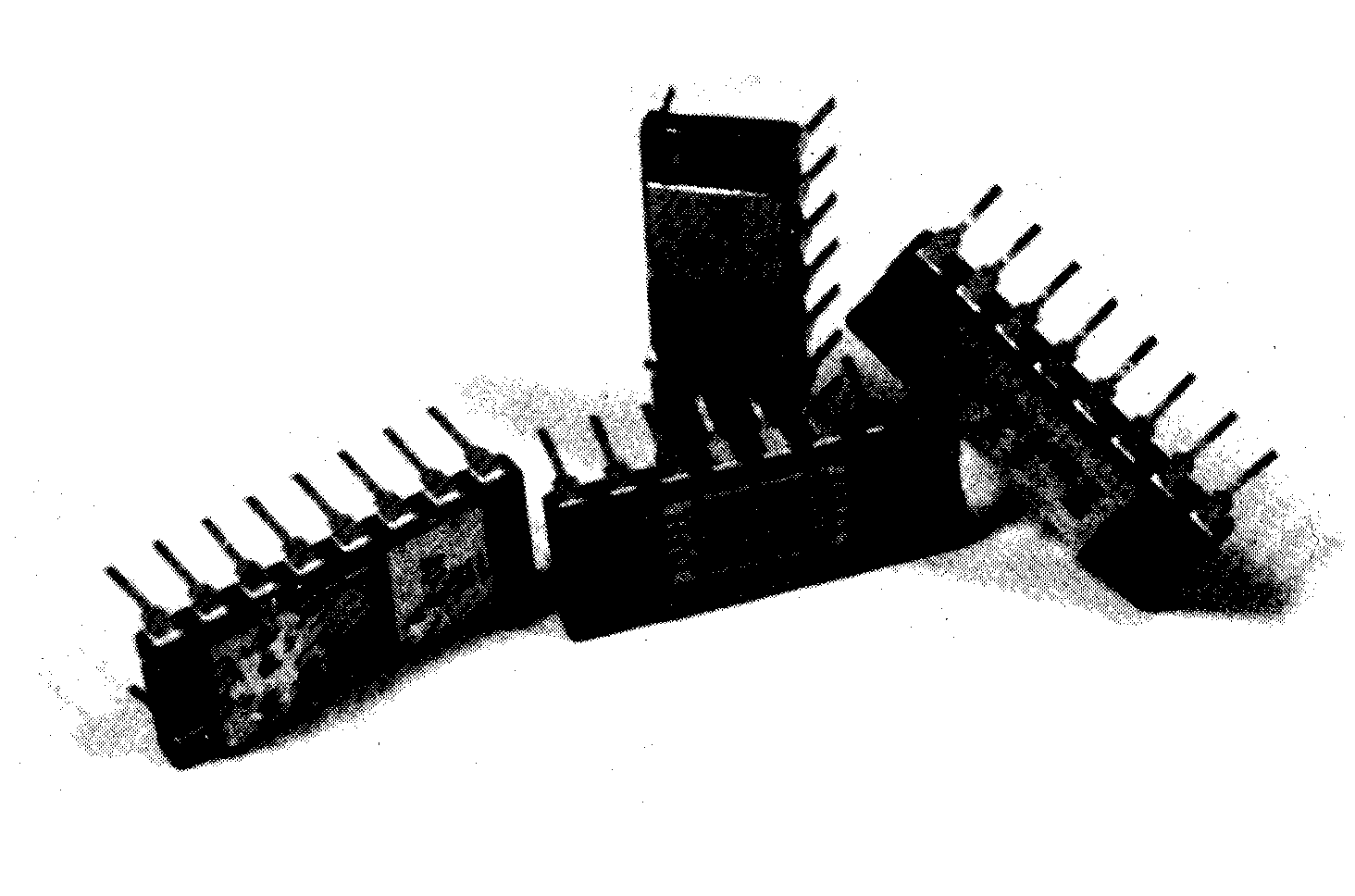
Taking the tops off 4116 DRAM chips proved to be quite simple, though you should be prepared to "write off" the first one you mutilate. There are a number of things which can go wrong (and did go wrong in the case of our prototypes). However, if you have a steady hand and follow the instructions, then all should be well.
The design of chip which should be used is the type known as Ceramic Dual-in-line Welded Seal. The pins are side brazed and gold-plated, which although not important, makes the chips easy to recognise. The body of the IC is usually grey in colour and a metal plate is soldered or welded across three-quarters of the top surface. The ICs used in the prototype bore the code HYA4116 A3. The metal plate has to be removed. The first attempt involved using a fine-toothed saw, with the IC already soldered on a piece of Vero board to keep it rigid. This worked, but put fine swarf and foreign bodies. onto the surface of the chip which then had to be blown off. In fact the solder/weld line is so thin that the plate can be cut and prised off using a Stanley-knife and this method produces hardly any loose material. Heating the plate with a soldering iron until it slips off also proved successful. On the exposed chip surface the two rectangular banks of cells making up the memory array can clearly be seen, as can the fine wires connecting the chip terminals to the IC pins. Contamination on the chip should be blown clear. Any brushing is likely to disconnect one or more of the fine wires.
Having exposed the entire chip surface, the next job is to cover part of it up again. Surrounding the memory matrix are all the address latches, address decoding and buffer gates and if light falls upon them they will fail to control the memory matrix properly! A good lens system would ensure that no stray light endangered the control part of the chip. We tried paint as a covering agent but that was difficult to apply accurately, so in the end the sensitive chip areas were masked off using part of the metal plate. Soldering it back onto the IC resulted in undesirable flux splashes so finally it was glued back.
A small convex lens was positioned in front of the IC so that the chip surface lay in the focal plane of the lens. Figure 2 shows how to find the focal length of a convex lens. In view of the fact that pieces of cardboard and plastic tape held the "lens,, in front of the "camera", it was perhaps surprising that any images were obtained at all. It will be very interesting to see what standard of results a school science department can achieve.
Suitable DRAMs can be identified by their packaging and the metal plate, once removed, reveals the capacitor array. The author's initial attempts at chip surgery proved less than successful.
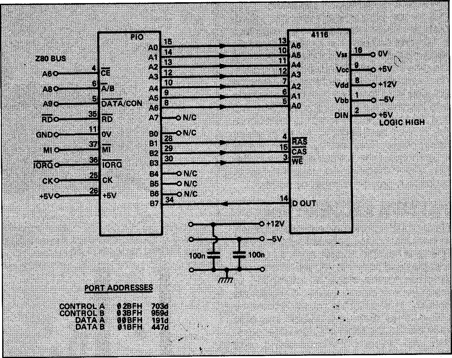
Figure 1. The hardware of the Solid State TV camera consists simply of the DRAM image sensor itself and a Z80 PIO.
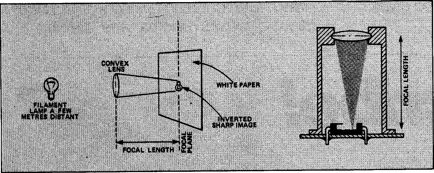
Figure 2a (left) shows the method used to determine the focal length of a convex lens. A piece of white paper is moved back and forth until an inverted image of a filament lamp some distance away is brought into sharp focus. The distance between the card and the lens is the focal length.
Figure 2b (right) shows the lens mounted such that an image is formed on only one half of the DRAM's capacitor array.
CONTROLLING THE CAMERA
The logical arrangement of the memory matrix of any RAM chip can usually be gleaned from its specification sheet. In the case of the 4116 the 16384 memory cells are configured as a 128 x 128 array which implies a nice square area of chip surface to receive the light rays. Unfortunately the physical arrangement of the matrix might not be so convenient since the manufacturers never intended it to be used as a solid state camera! The 4116 is physically separated into two rectangles of 64 x 128 creating a sizeable “blind spot" in the corridor between the two rectangles. In fact the solution is to focus on just one rectangle, and the program thus processes 64 x 128 - 8192 image points, and puts them out on the screen as Spectrum pixels in ink or paper colour. This seemed reasonable for a prototype. Later versions using a better lens and 4164 memories could attempt to process a greater number of points.
PATTERN RECOGNITION
Having built a prototype camera which will at least distinguish between light and dark and "see" simple shapes such as circles, triangles and squares, you will now wish to progress to the stage of attempting to teach your computer to recognise simple shapes. In a series of recent articles by Mike James (February, March and May 1983 E&CM) the topic of Pattern Recognition was given a thorough airing, and sample programs to run on a Spectrum were given to illustrate the points made. The programs work without the need for hardware devices since they are illustration theory rather than proving practical applications. Mike James supposed that a low- resolution light-sensitive device might be built for tens of pounds... Now you have one for under a fiver!

Even fairly crude lens mounting arrangements can give acceptable results yet care taken in this area will give the best results from the system.

The author's test card (above left) was kept fairly simple. A typical image produced by the system is shown above right.
Next Month...
Software listings for the camera.
Discussions
Become a Hackaday.io Member
Create an account to leave a comment. Already have an account? Log In.