 kittan
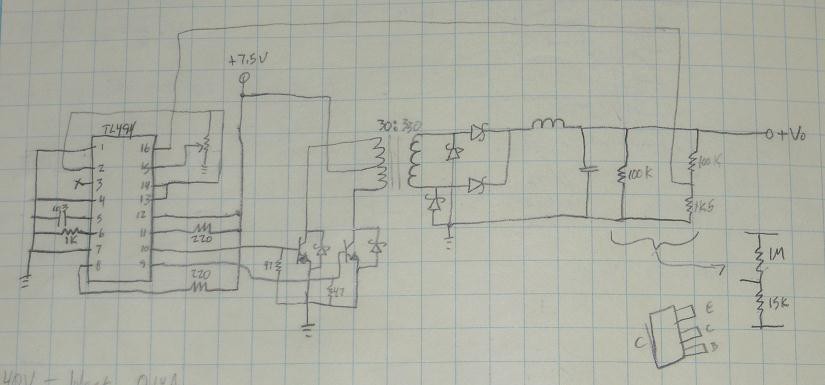
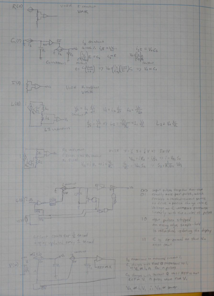
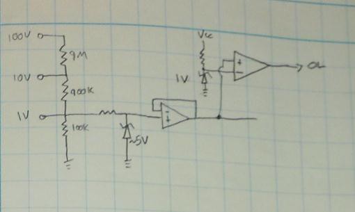
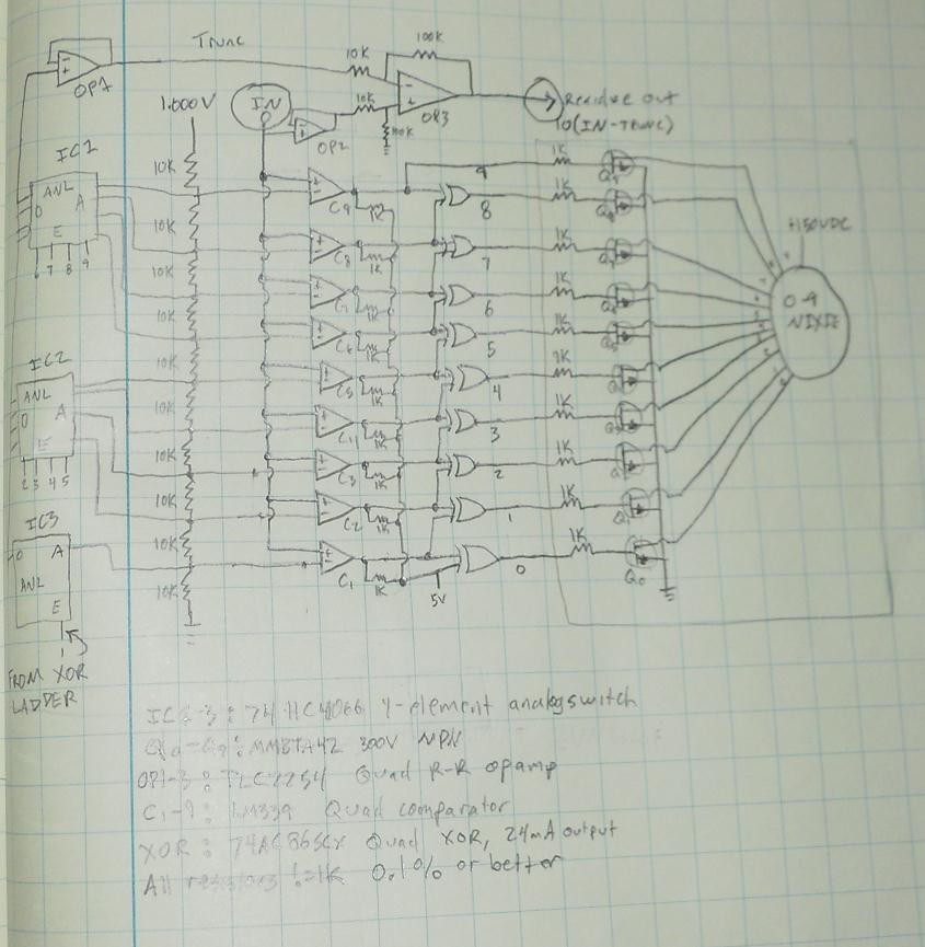
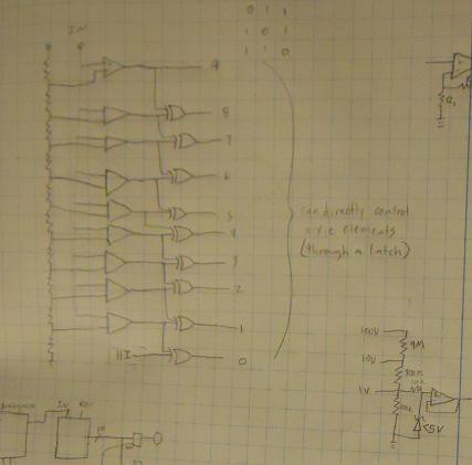
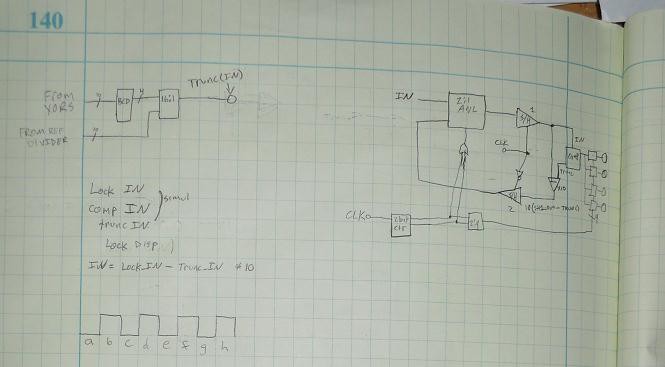
The purpose of this project is to build as diversely functional multimeter as possible, using as little digital electronics as possible. At times it will be required to use something like a single 555 or basic logic, but nothing with nested or combined logic will be allowed (except minimally where it might be required for latching states for a particular type of measurement, or to hold display outputs for readability). No microcontrollers will be used, no self-standing ADCs, no BCD converters, nothing. As much as possible what can be done with just analog circuits (opamps, etc) and discrete passive components (R, C etc) will be done with them only.
Don't even think about telling me to use an Arduino. You will be slapped.
0%
0%
State-Based Nixie Digital Voltmeter
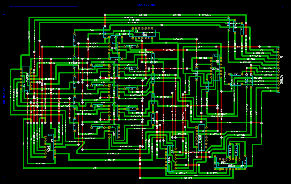
A digital voltmeter built without any microcontrollers or integrated ADC chips. Based entirely around discrete logic and comparator ICs.
Become a Hackaday.io member
Already have an account? Log in.
Just one more thing
To make the experience fit your profile, pick a username and tell us what interests you.
Pick an awesome username
hackaday.io/
Your profile's URL: hackaday.io/username. Max 25 alphanumeric characters.
Pick a few interests
Projects that share your interests
People that share your interests
 John Duffy
 NNNI
NNNI
 James Wilson
 Paul Andrews