Close
0%
0%

uPD7220 Retro Graphics Card (and VGA hack)

Making an 80s GDC run for the first time in decades, and my first real hack on hackaday.io

Public Chat
Similar projects worth following
The uPD7220 is a fascinating chip from the 1980s. It was meant to control CRT displays and provide graphics capabilities, but I have found a way to make it output a valid VGA signal.

It is really complex, so understanding it takes a lot of studying of the sparse available information (and virtually no example code), but most certainly worth it. I intend on sharing my understanding and lessons here so more people can more easily use this awesome chip!!!

I plan on posting more on this when I can!

Resources

Datasheet: http://www.vintagecomputer.net/fjkraan/comp/qx10/doc/nec7220.pdf

This is best used for designing a circuit with the uPD7220 and for understanding how to initialize and draw with it.

Programming Manual? : http://www.vintagecomputer.net/fjkraan/comp/qx10/doc/nec7220.pdf

This will explain how to send commands and generally how the CPU to uPD7220 interface works.

My Z80 code: https://github.com/NuclearManD/z80-code/blob/master/G00nOS/upd7220.z80

This is the graphics driver I am writing for my Z80 computer.  It's good example code, but it currently has numerous limitations, so look at the arduino sketch I uploaded to this project as well.

Why?

I want a graphics card for my Z80 computer so it can operate completely independently, as in, without a serial monitor.

I don't want to use a propeller chip or other powerful microcontroller because those chips don't go with the rest of my Z80 computer.  Besides, something about this design just feels really... pure, I suppose.  Clean.

NOTE: The information provided in this details section is very condensed.  There is much, much more to be understood.  I recommend STUDYING the documents I linked and uploaded.  The following information is just a brief overview.

How does the hardware work?

The uPD7220 generates VSYNC, HSYNC, and BLANK signals.  It generates a few other signals for the memory interface, but these must be interpreted.  The uPD7220 address and data lines share a bus, so the address has to be latched.  Also, to write to memory, there are special cycles which require external hardware to generate a write enable.

There are two clocks.  The pixel clock, which is currently 8Mhz, is used to output pixels.  The uPD7220 takes lower frequencies, so the pixel clock is halved to make the 2xWCLK clock, which is sent to the uPD7220.

The uPD7220 reads the pixel data onto the data bus, where it is latched every fourth pixel clock rising edge.  The shift registers output pixel data while the uPD7220 prepares for the next set of pixels.

The port which goes to the system microprocessor is directly connected to the uPD7220, except for two OR gates which generate the WE and RD signals.

How does the software work?

There are two ports that can be written/read on the uPD7220:

READWRITE
0Status registerParameter load
1Data to CPU FIFOCommand load

Before each write, the status register FIFO full flag must be checked first.  If the FIFO is full, then a write will create undefined behaviour.

The uPD7220 must be initialized properly first.  If it is not initiallized right, then random commands will crash it when it is least expected.  These commands all must be used in initialization:

0x00 : reset (followed by graphics parameters)

0x47 : pitch (aka tell the GDC the number of horizontal words there are per line)

0x70 : set up PRAM so drawing operations work

0x4B : CCHAR : set up character parameters.  

0x46 : set the zoom.  Otherwise zoom may be random.

0x6B : start the display!  YEET!

uPD7220_card_v2.zip

The v2 design. It should work as intended, based on simulations.

Zip Archive - 1.22 MB - 06/12/2024 at 19:00

Download

updgfx_r0.kicad_pcb

KiCad raw PCB design. This can be uploaded directly to OSHPark.

x-kicad-pcb - 1.89 MB - 05/08/2024 at 01:52

Download

updated_uPD7220_design.zip

Updated schematic, with all KiCad design files. This is a bit messed up due to the KiCad version change and transfer, but the PCB design should work fine as is. This fixes the connections to the color resistor networks, and fixes the oscillator.

Zip Archive - 3.62 MB - 05/08/2024 at 01:51

Download

updgfx_r0_updated.pdf

Updated schematic, provided in PDF format. This fixes the connections to the color resistor networks, and fixes the oscillator.

Adobe Portable Document Format - 138.46 kB - 05/08/2024 at 01:50

Preview
Download

video_timing_calculator.py

Python3 program to create valid VGA video timings for the uPD7220. Use it to generate values to plug into videoconf.h

plain - 5.11 kB - 04/04/2019 at 06:05

Download

View all 9 files

  • 1 × Z7220 Super Rad 1980s GDC, clone of uPD7220. The Z7220 is fast enough, the original isn't
  • 4 × 74173 Logic ICs / Flip-Flops, Latches, Registers
  • 4 × 1k Resistor
  • 1 × 10k Resistor
  • 1 × 8,10, or 12 Mhz DIP8 Oscillator

View all 13 components

  • Card Design Fixes and the Simulator

    Dylan Brophy3 days ago 0 comments

    I spent an all-nighter making a simulator for the card, which can load the schematic from KiCad, then spent an egregious amount of time in the sim making the card work.  As promised last log, I will show a bit more on the simulator:

    For those that prefer reading over watching, I'll do some brief explanation of the simulator, then go over the card itself.

    About the Simulator

    The simulator loads the KiCad PCB file, constructing a netlist and list of components.  There's a (small) component library, which has a simulation model for each component type.  The simulator schedules chip updates based on each IC's propagation delay, so the simulator should be largely accurate from a timing perspective too.

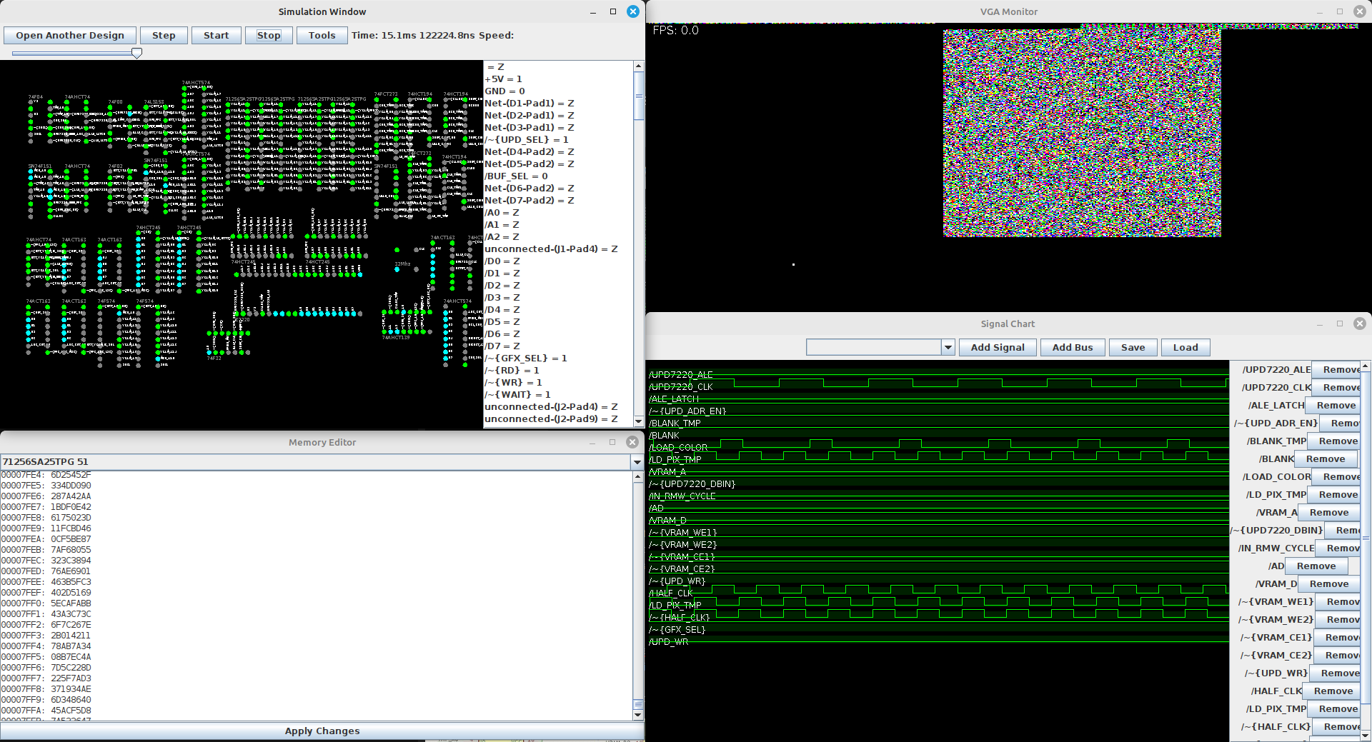
    The simulator has some handy features for graphics devices particularly, for example, a VGA display simulator.  In the picture, there is a white dot on the VGA display - that is the position of the electron beam at this particular tick.  The sim was definitely engineered to my particular use case.  Well, I'm pleased with it and hope to use it in projects in the future.  Now I can know if a board will work before I order it.

    The simulator uses a lot of bit manipulation, and for this reason, it does not at all support analog signals at this time.  It's great for simulating logic chips and RAM - or really any ICs that are digital.

    I also connected the simulator to my Teensy 4.1, so I could run a simulation with the software in the loop.  You can see that in the video up there as well.

    Oh, what is that I hear? You could have just used an existing simulator!!  Really?  Huh, I guess that didn't seem fun enough, well, too late now anyway.  Well, here's the source code, if it is wanted: https://git.nuclaer-servers.com/Nuclaer/kicad-logic-simulator
    But also, I don't think an existing simulator would have all these features I wanted, and honestly, building this sim didn't take *that* long.  I'm really amazed I did it as quickly as I did; I would have expected it to take at least twice as long to write a program like this.

    I love MUXes

    I replaced many of the logic gates with MUXes, as it is a lot easier to understand what the logic is doing, and the logic is just so much more flexible this way.  I got the idea from LUTs in FPGAs, which work in a very similar fashion.  The MUXes can accept quite a lot of inputs if you're creative, since you have select lines, enable lines, and inputs - this can afford you a lot more logic per chip than logic gates.

    3 of the 4 MUXes my deisgn uses now
    Changing the RAM

    I think I went over this in my last log but I don't remember; well, I needed to change the RAM ICs.  The speeds on this board are extremely fast, with a maximum of a 32Mhz pixel clock.  I needed RAM that could read/write in less than 30ns for the card to have the whole display written fast enough from the Teensy (or whatever other device).  Hopefully I did my math right because I already made the card use different RAM ICs, and these are blazing fast, at 25ns.  Unfortunately, this dramatically reduces the maximum graphics memory, which is now 128K (up to 262144 pixels).  These numbers are halved if you use hardware double buffering.  This limits the highest resolutions to 640x400, or 540x480, for example.  This bothers me, so maybe I'll have to make an upgraded card in the future.

    For reference, here is the RAM chip I'm using now: https://www.renesas.com/us/en/document/dst/71256sa-datasheet

    Schematics and Other Details

    I think the design will work, based on the simulation, so I'm finally uploading the schematics after this log is posted.  This time I'll add the component libraries and such too, so there will be less issues a few years from now in KiCad 11.0, or whatever will be brewing by then.

  • Problems with the New Version - and a Simulator

    Dylan Brophy06/03/2024 at 23:01 0 comments

    My board design had a LOT of problems.

    Let's take inventory of my mistakes, so you can hold them against me:

    • The address connections A16 and A17 from the VRAM to the uPD7220 were not set up completely right, causing a strange monitor flicker in mixed mode, and lack of memory access if the software didn't have a special setup
    • VRAM control lines were not generated correctly
    • The VRAM was not fast enough to do what I had in mind.  I thought I checked this and I knew the timing was close, so I must have done my math wrong.
    • Probably something else I forgot

    I thought there might be a minor issue or two with the design, as the design of the VRAM access is very ambitious - accessing two words per cycle using careful timing, then switching what device controls the memory every other cycle.  Yes, a lot can go wrong.  But what I didn't expect, is that so much would go wrong.  I practically have to re-design more than half the board.  Well, that is more or less what I've been working on.

    Here's a video showing what the debugging was like; hopefully the video isn't too chaotic:

    At some point I realized that I couldn't figure this all out by messing with the hardware directly - there were just too many things wrong with the board.  The breadboard was losing me both signal integrity and voltage - the board ran at less than 4.3v.  I needed a simulator.  Well, I wrote one.  It works decently well, loads my schematics straight from KiCad, can show me the VGA video output, and has a few other random features.  Here's the source on my personal gitlab server, and here is a picture of it:

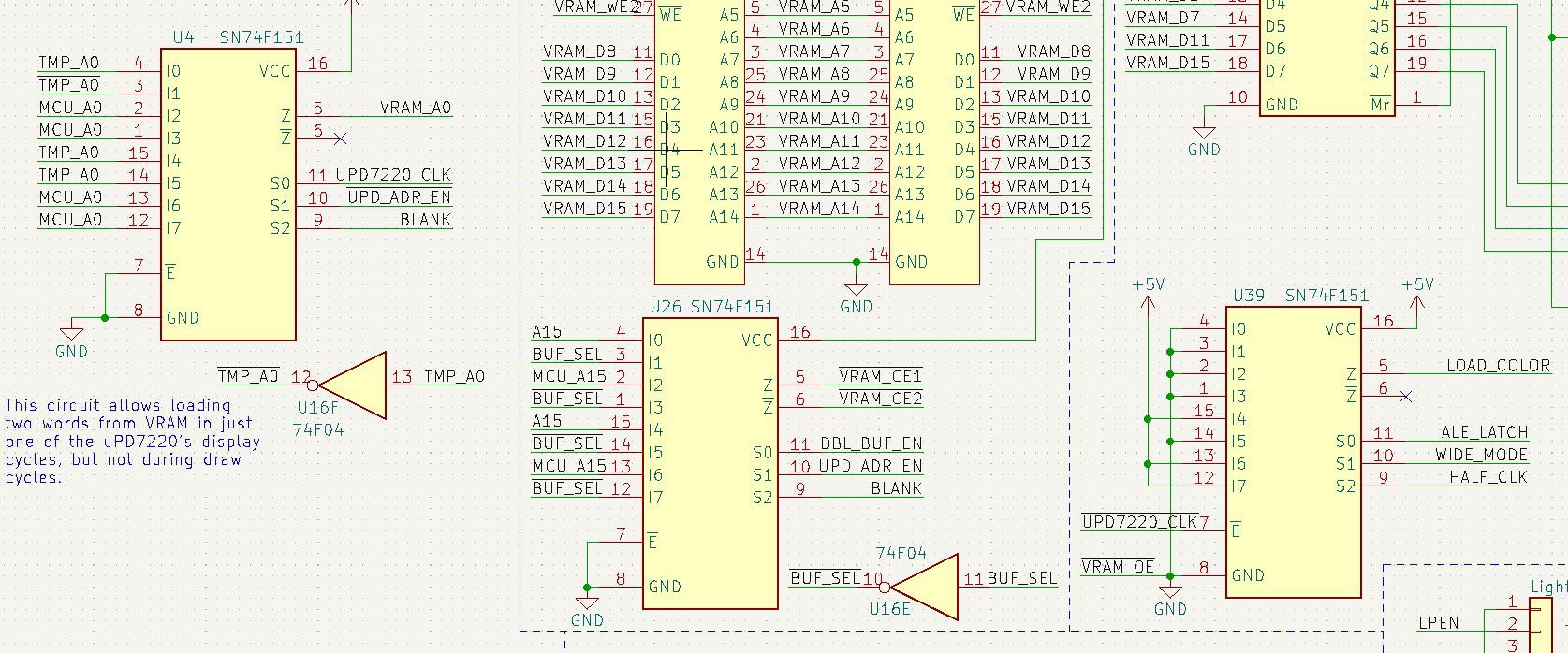
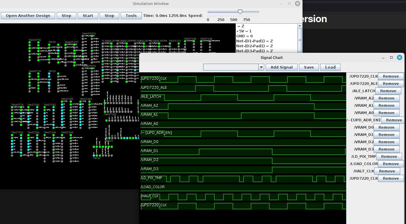
    It is VERY alpha, and the library of components is incredibly limited.  It has bugs and the UI can crash sometimes.  That being said, the simulation itself does not seem to have any problems.  It does just one thing extremely well: it simulates the card I'm working on.  With some relatively small upgrades it could probably be used to simulate a wide variety of digital circuits.

    In any case, I've been using this simulator to work on a fixed design.  This is still in progress; I'll post one more log when I order the boards, then I can try again when I receive the improved boards.  I'll go over my changes to the board in depth on the next log, but basically I've switched the SRAM ICs to 25ns chips so I can get the timing I want, and I've removed most of the logic gates and replaced them with MUXs to make something akin to LUTs - kinda like an FPGA with TTL, except the LUTs are hardwired.  Much easier and more reconfigurable than trying to use gates - and in some cases it's actually faster too.  Well, until next time.  Wish me luck on a fixed design!

  • V2 Board Design

    Dylan Brophy05/12/2024 at 01:12 0 comments

    KiCad 3D render of my board design:
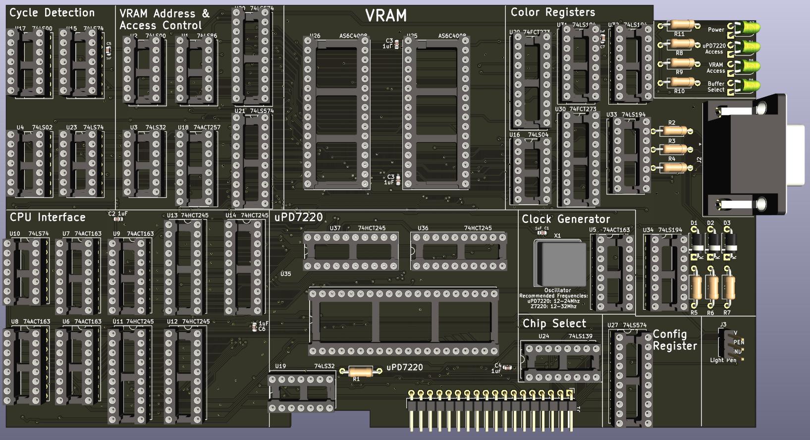
I tried to make the parts of the circuit clearly visible on the board.  I also added LEDs, which I typically forget when designing a board. Every board needs blinking lights. Well, I think this board has turned out nicely, at least in the 3D render; it has the clean look I wanted.
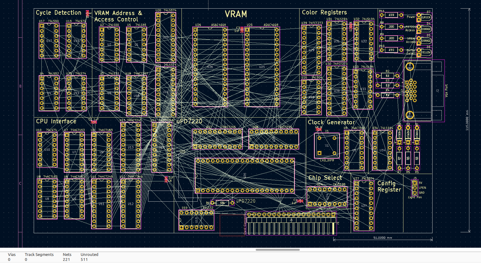
    Here's the ratsnest and basic layout before I routed it:The board now:
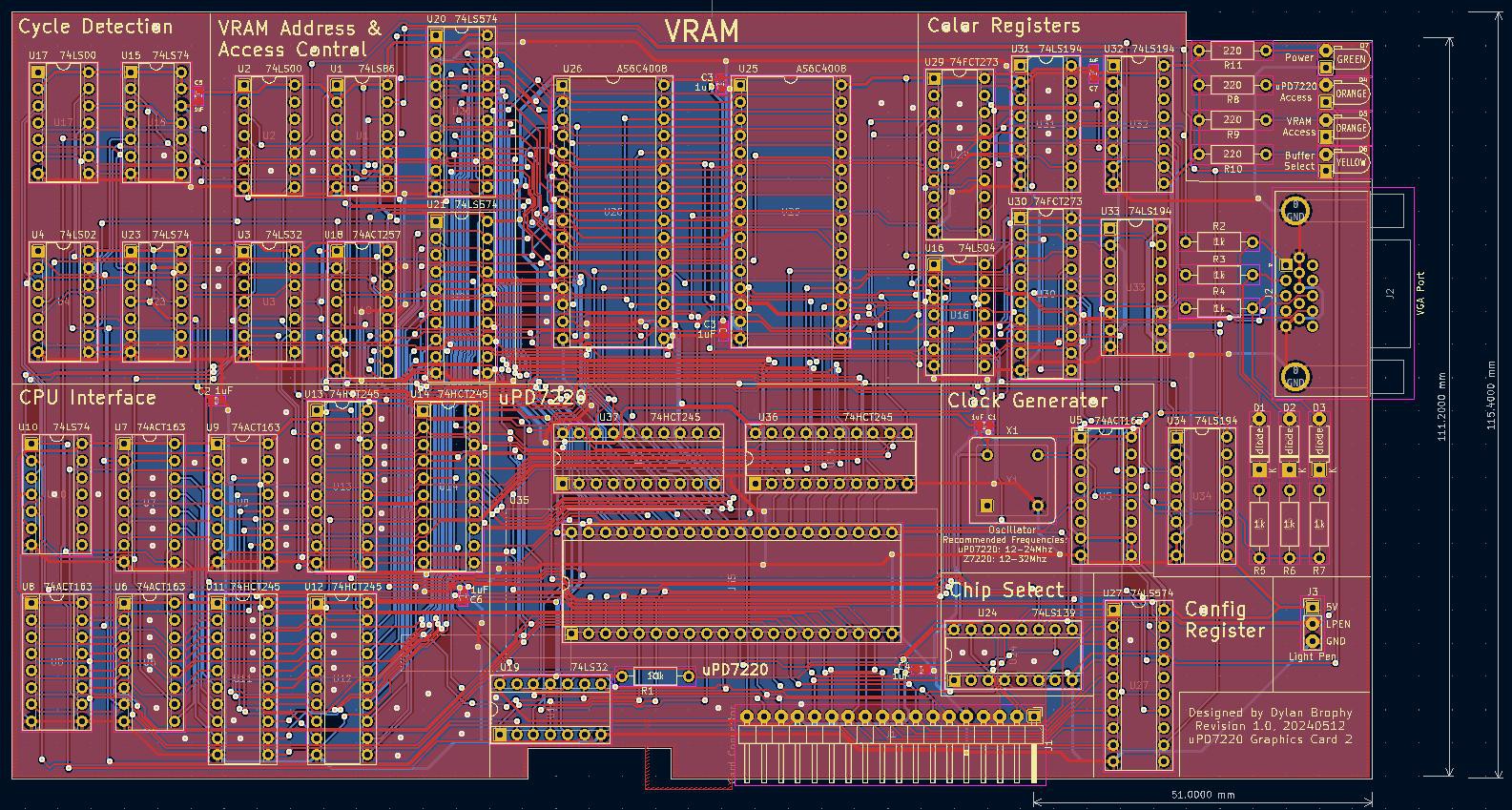
This board was a lot easier to route than I expected.  Anyway, expect an update in maybe 10 days when I actually assemble it.

  • V2 Schematic Ready

    Dylan Brophy05/11/2024 at 20:14 0 comments

    I have the schematic finished now.  I checked the major critical paths to the VRAM, fining one that was too slow.  The VRAM takes up to 55ns from address input to data output, and I have only 62.5ns, so really it is super close.  Since the uPD7220 uses an address latching mechanism, I managed to move my address-modifying critical path to before this latching is done.  The timing there is much more forgiving.  Other than that, I added some pretty LEDs and checked/fixed some of the logic done in the circuit.
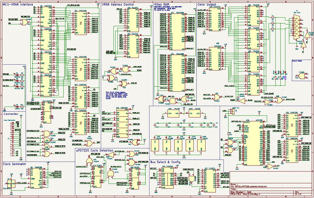
I may add more decoupling capacitors still, but that isn't a real design change.  The capacitors are the only SMD components I'm using.

    In total I'm using 32 TTL ICs, two RAM chips, and the uPD7220 of course.  Loading it in the PCB editor, it looks smaller than I may have expected, but I don't think I'll feel the same when I receive the finished board - it is significantly bigger than my original uPD7220 card:I think I'll also need to make some minor adjustments to the circuit design so the routing is easier, but these are not really functional changes - things like changing the bit order on registers, or rearranging the allocation of gates from chips.

  • New Schematic is Nearly Complete

    Dylan Brophy05/10/2024 at 18:55 0 comments

    My schematic so far:

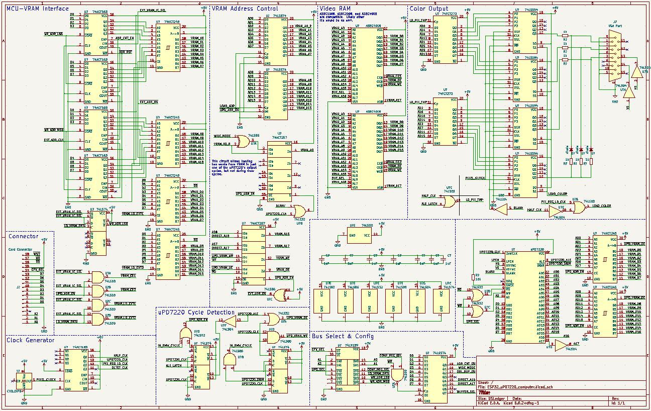
    This schematic is way better organized, and hopefully it will still make sense to me 5 years from now.  I've added a ton of features since the last board revision, namely:

    • The CPU can now directly access the VRAM
    • I doubled the maximum pixel clock by allowing for uPD7220's wide mode (see last log)
    • Added support for double buffering
    • I octupled the maximum VRAM to 512KiB from 32KiB.  Now we can have larger resolutions with enough RAM left over to double-buffer

    Doing all this added a TON of extra logic, so if you compare the above schematic with the schematic of the previous board, this one has at least twice the components, and is far denser.

    I had to add a lot of buffers so that the VRAM bus could be shared.  This concerns me because it adds a few tens of nanoseconds to certain datapaths, meanwhile I've doubled the maximum VRAM clock speed to 16Mhz.  The VRAM uses 55ns alone, and that doesn't count any of the hardware for uPD7220 memory cycle detection, bus sharing logic, etc.  So the next step will include checking my datapaths to make sure all the components process fast enough for my clocks.

    Here is some of the new logic for handling the communication from the main processor directly to VRAM:
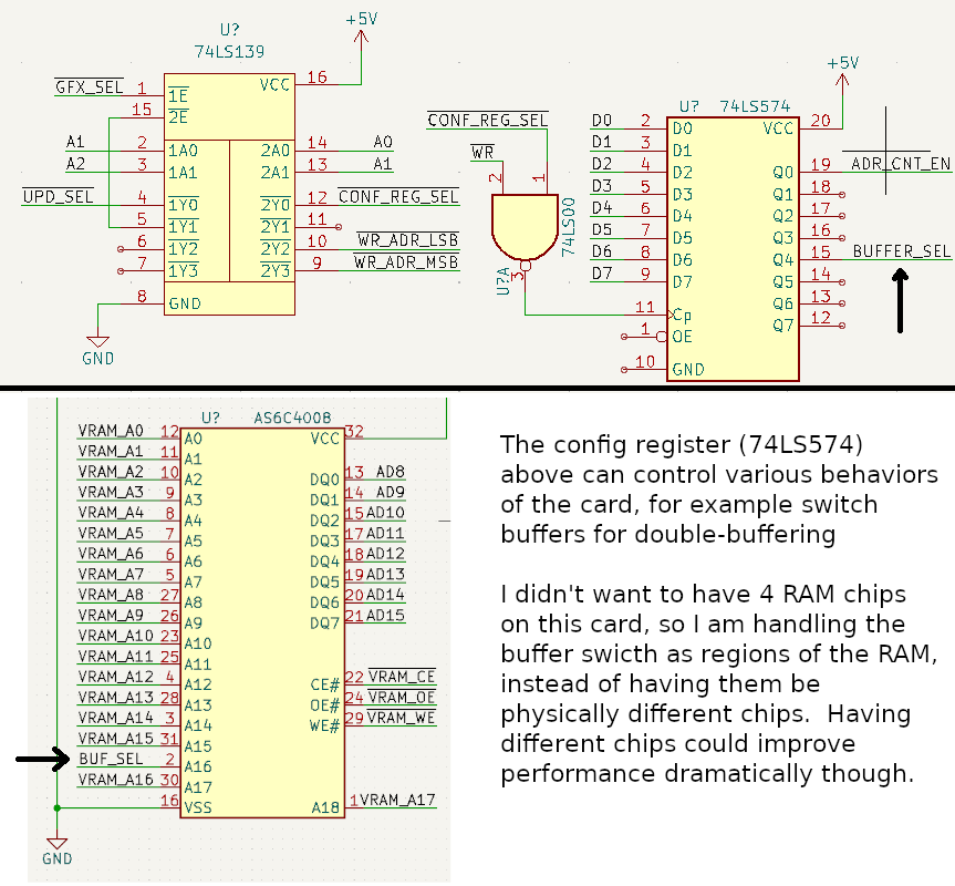
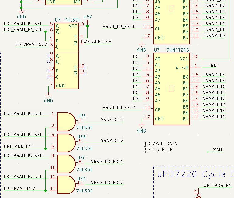
Some of this logic is wrong I think, namely I'm suspicious of the two bottom NAND gates, and I need to add logic for the WAIT line, but this image should give some idea of what the logic is supposed to do.  After the main processor writes the lower address byte, the byte-select for the VRAM is reset to zero.  Then the processor can write a single byte to the VRAM, which automatically switches the selected byte so the processor can write the other byte.  This is done because the VRAM has a 16-bit bus and the processor has an 8-bit bus.  Depending on weather the address counting is enabled, the address registers will actually count up to the next word in VRAM, so that the processor can send up to 128KiB of uninterrupted data to VRAM.  This is done in-between accesses done by the uPD7220, as the bus is shared, and the uPD7220 gets priority.

    The exact behavior of the board's logic is controlled by a special control register I added:
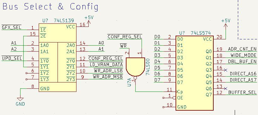
I realize now, looking at this, that I may be able to remove a latch by using A0 for byte select instead of automatically selecting it.  Something to think about.  Anyway, in the image above you can see that the config register can enable/disable the wide mode logic, control automatic address count, enable or disable double-buffering, to swap buffers, and set A16/A17 for direct VRAM access.  The double-buffer enable will make the uPD7220 and processor write to the opposite buffer as the one being displayed, but the buffer still must be manually swapped by the processor.

    Anyway, this is where I'm at now.  The schematic isn't quite finished, once I finish it and have the board design I'll upload the files to the project.

    [edit] bonus: falstad simulation of part of the circuit responsible for loading pixel data from VRAM and clocking it out, which allows wide mode:  Simulation

  • "Wide display mode"

    Dylan Brophy05/09/2024 at 16:20 0 comments

    I found part of the datasheet discussing "wide display mode", which tells the uPD7220 to skip an address each time it loads a word to be displayed.  Here are the relevant sections of the datasheet:
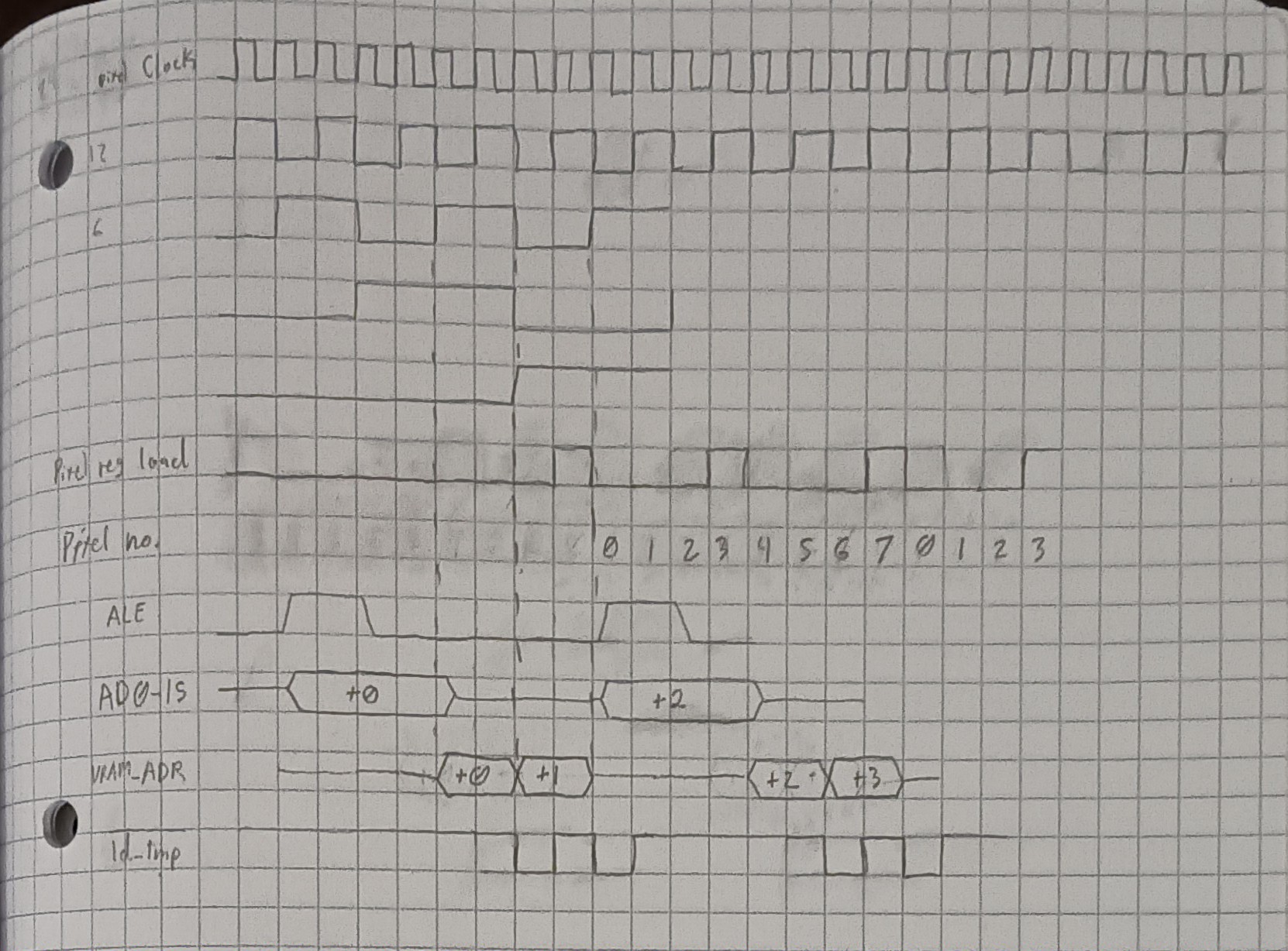
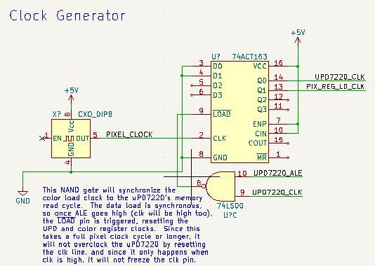
As it turns out, I don't think I can get it to add 4 instead of just adding two as described above; this limits my maximum clock speed to 24Mhz (32Mhz on the faster Z7220), so the maximum resolution would be limited by this.  On the other hand, the uPD7220 supports interlacing, so I might be able to push out a higher resolution that way.  Without interlacing under this config, I can't even get to 640x480, but with interlacing I can get at least to 720x480.  I'll have to play with the settings.

    I'll need to add a 16-bit register to handle this, since I don't have a real 32-bit bus to load color data from:
    I still need to add the logic to generate LD_PIX_TMP, which requires detection of the uPD7220's memory cycles.

    The waveforms should look something like this:

    The clock at the top is the pixel clock, the fastest it can do is 4x the max GDC clock (so 24Mhz for uPD7220, 32Mhz for certain Z7220 variants).  The third clock from the top is the GDC clock.  The color shift registers load every fourth pixel clock, shown on the 6th signal down from the top.  Each GDC memory cycle we will now be loading 8 pixels instead of just 4, so you see the pixel number reflect this.  Once the address is latched, we can load two words in succession, at twice the GDC clock speed.  To do this, we use the 16-bit register previously mentioned, which loads twice during this single GDC memory cycle, once for each 16-bit word.  The first time it does this, the color shift registers are immediately loaded, thus saving the color data for the first four pixels.  This way, the same 16-bit register can be reused to save the next word.  The LOAD signal to this register is shown as the active-low signal on the bottom of the image above.

    Here's the logic I designed to generate this waveform:
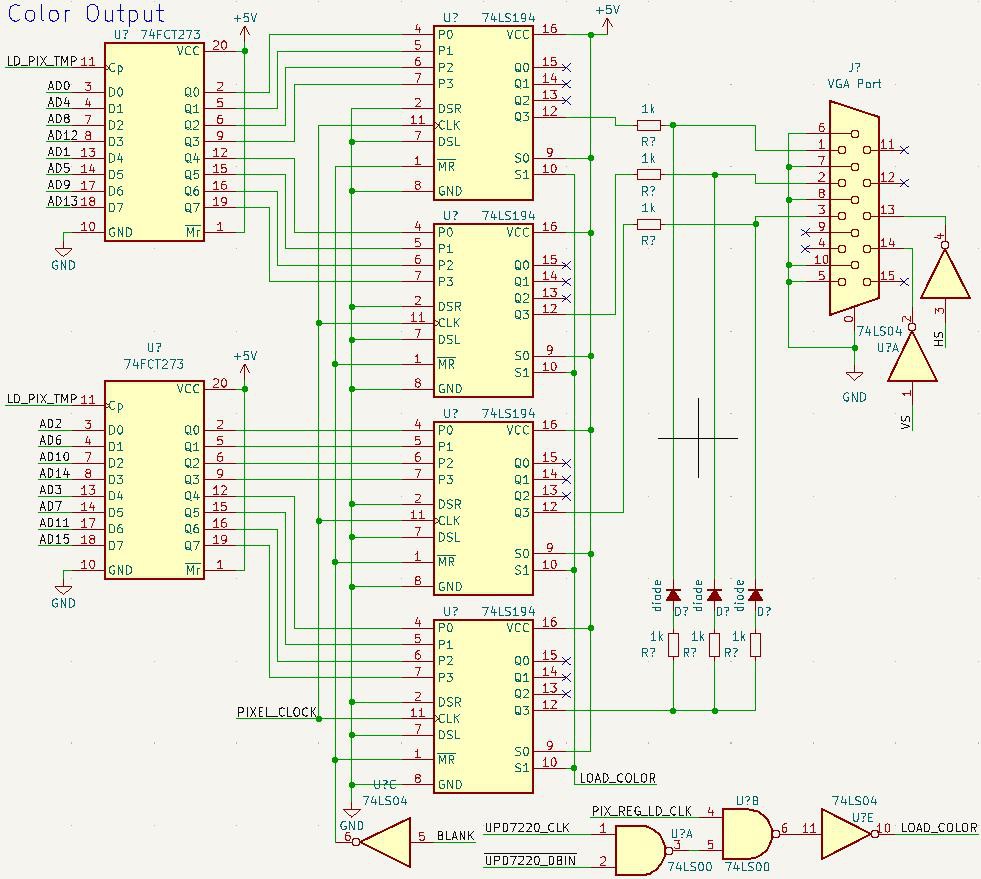
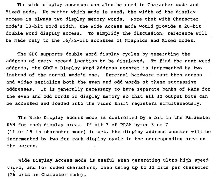
    As a bonus, I'm including a timing diagram from the datasheet so it is easier to find later:
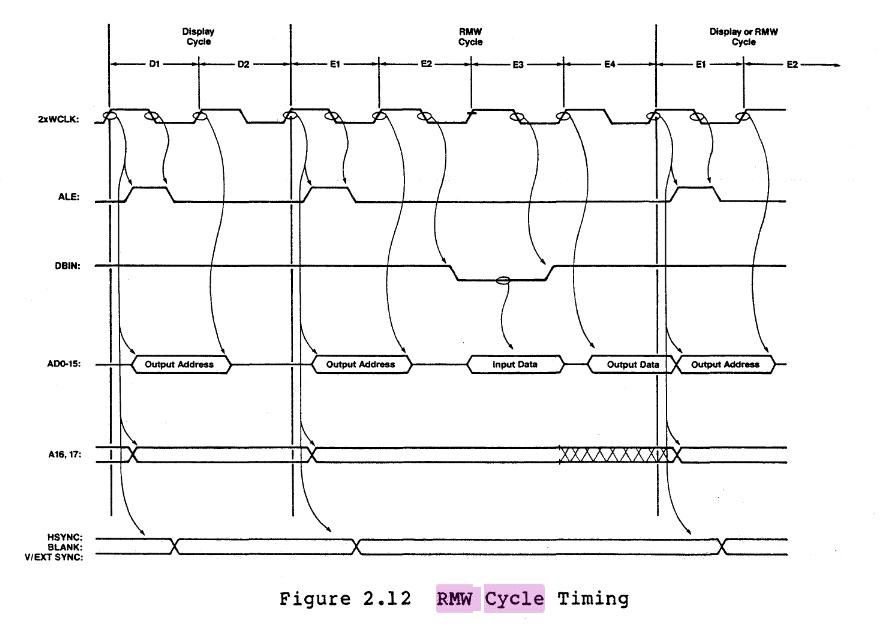
This image details the cycles of various uPD7220 memory accesses, and is super useful for designing the memory control logic.

  • We can certainly make this better.

    Dylan Brophy05/09/2024 at 15:39 0 comments

    I hadn't looked at this project in a long time, and the other day I was browsing it and noticed several comments asking for the schematics. But hadn't I uploaded schematics?  So I double checked the files, found the attached schematic zip, and decided to open it up.  Oh geez, what a mess!  It had been created with a very old KiCad version compared to today, and I don't think I uploaded the symbol libraries, so the schematics were useless.  I can see now why people asked for the schematics!Broken schematic

    Very useful indeed. (not)
    I spent some time the other day cleaning this up, as well as fixing a few hardware bugs related to the color DAC and oscillator.  I modified the schematic to match the modifications on my board at home, which works quite well.  Here's the schematic now, which I uploaded:
    Repaired schematic
    A lot better, but still messy.
    The wires are very messy, consistent with how I made many schematics in highschool.  Clearly, this schematic needs to be redone from scratch.  Well, if I'm going to redo the schematic and roll a new board, why not make a bunch of improvements too?  Well, this is exactly what I've been working on.

    Upgrading the board
    If you saw my log in #Arduino Desktop, then you'll know that I mentioned this project, in that I may want to add it to another Teensy or ESP32 based computer system.  A Teensy 4.1 could write a lot of data to VRAM very quickly, which would be great for drawing bitmaps, and in-between the uPD7220 can draw other shapes.  In that log I also mentioned double-buffering the uPD7220, so there would effectively be two RAM banks, which could be switched by some command.  To my knowledge, the uPD7220 does not support this, so I needed to add the logic myself.  I'm still working on the schematic, but here's where we are so far:
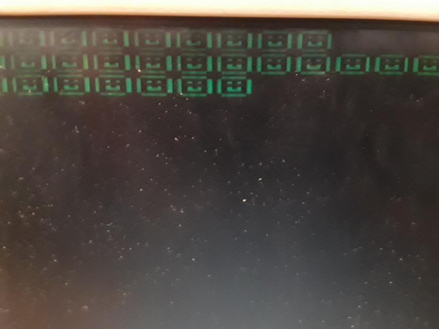
I'm not a huge fan of the old board's low resolution.  I want at least 640x480, if not higher.  Adding more memory for this is quite easy, and in the new schematic this is already handled - the hard part is getting the clock speeds high enough.  The uPD7220 can clock at 6Mhz, and the current card gets this by dividing it out of a 12Mhz clock.  With a Z7220 the clock is a bit higher, 8Mhz and 16Mhz respectively, but this is nowhere near the pixel bandwidth needed for higher resolutions.  My solution to this will be to divide the uPD7220's clock one or two times so we can get 24Mhz or 48Mhz pixel clocks on a uPD7220.  That should allow us to get way better resolutions:
    I really hope I'm using this calculator right.
    The 800x600 resolution in the above image is a good spot, and uses about half of the VRAM, leaving the other half to be used for double buffering.  I haven't made this part of the circuit yet, and one big thing I'd need to figure out is how to get the right signals to the VRAM for loading the pixels.  I could generate the VRAM's A0 with some logic to load two words out of VRAM each time the uPD thinks it's loading one, but this introduces an issue where the uPD would not be able to draw graphics to half of the pixels.  Perhaps there is a way to have the uPD skip a word each pixel load, then simply modify the A0 line to load this way?  I don't know yet, I need to consult the datasheet and see how this type of thing was done in the past.  I have a feeling they may have used two uPD7220s for this type of thing, but let's see if we can do it without that.  The chips are rare, after all, and the Z7220s are even more rare.

    Here is the current clock generator circuit for the new board, which should behave exactly the same as the old board; its job is to generate clocks for the board and to control when pixels are loaded into the output buffer:
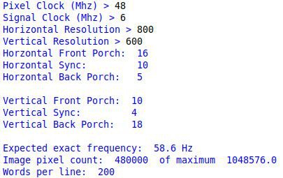
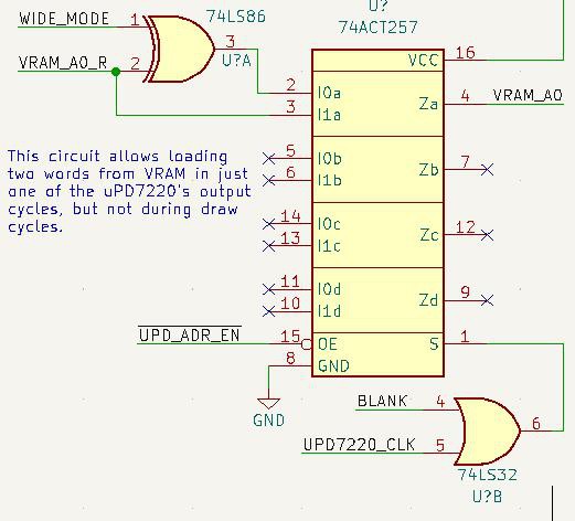
    Anyway, I have more stuff to figure out with the board.  If any of you have good ideas on the clocks and loading twice the pixels from RAM, let me know :)
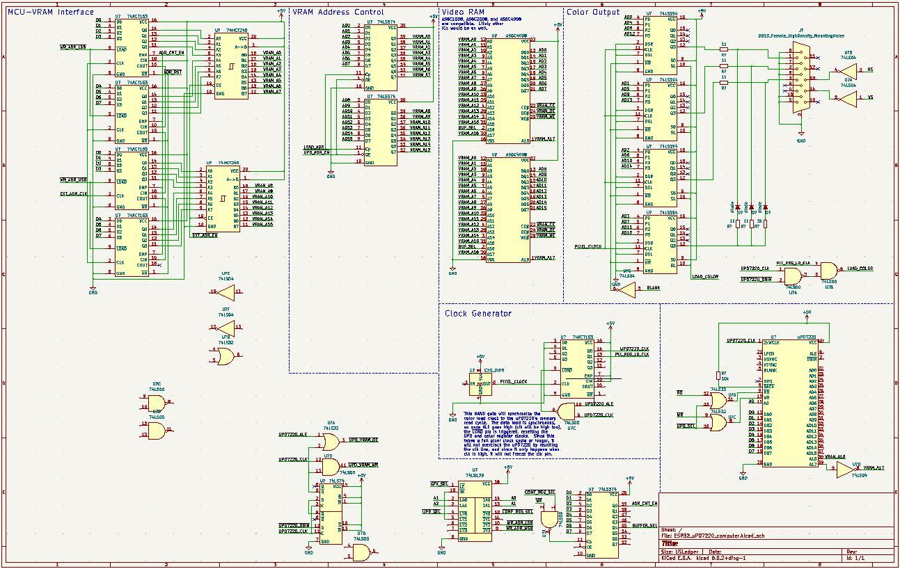
    Hopefully my schematics are prettier and more useful this time; I think they will...
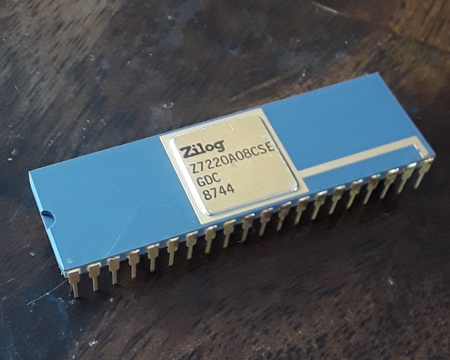
    Read more »

  • Zilog Made a Clone!

    Dylan Brophy04/18/2019 at 01:47 0 comments

    I bought this chip off of Ebay.  It seems that Zilog created a uPD7220 clone - and it works!  These chips seem to be rather rare and information on them is scarce.  I did manage to deduce that there were two variants of chips:  one operating at 6Mhz, and one at 8Mhz.  I got the 8Mhz one and tried doubling my pixel clock to 16Mhz (the GDC uses a halved clock).  That worked too, and that allowed me to make a more stable video signal.  I had a problem with the 8Mhz pixel clock where there was not time to output a valid video signal.  Now I can output more pixels than I have VRAM for.

    The chip is also a super pretty Zilog gem <3

  • Rendering characters!

    Dylan Brophy04/05/2019 at 19:41 0 comments

    I've managed to make my card render characters!  I used the Z80 computer this project was originally intended for this time, instead of the Arduino testbench.

    There is not a font yet, so I just rendered a bunch of smiley faces and tested that the program could keep track of the cursor position.

    Smiley faces are a good way to do testing.

    It's working very well, but I would like to render things a bit faster.  I think the Z80 math routines run slow however, for calculating cursor positions and colors.

    It doesn't help that my card has 16 colors - it appears that the uPD7220 was designed to just do black and white.  This means that I have to send a few more commands to the uPD7220 to select a group of bits for a pixel (multiple colors) instead of just one bit (black and white).  The uPD7220 automatically selects a single bit when a command is sent to set the VRAM address, but my program must select multiple.

    Here is my graphics driver for the Z80: https://github.com/NuclearManD/z80-code/blob/master/G00nOS/upd7220.z80

    You may need to look at some of the other files, but all graphics functions are there (er, rather, the ones I've written thus far).

  • Finally on HaD after more than a year! And finally working!

    Dylan Brophy04/04/2019 at 06:29 0 comments

    Over a year ago I wanted a graphics card for my Z80 computer.  I made a prototype with the uPD7220, but I never got it working.  Until...

    As it turned out, I made TONS on mistakes in the original design.  There are issues with the new design too, but it works well enough (after a hack, more on that later). Anyway, after playing with the first prototype and trying various hacks, I ended up with a valid VGA signal!

    I don't think the uPD7220 was ever supposed to output VGA, considering VGA was introduced about four years after the uPD was, so it's awesome that it can output a VGA signal.

    After studying the uPD datasheet and my schematic in depth, I eventually found most of the problems and ended up with my second prototype (which I am using now).  I've managed to get it to do the basic things I need it to do.  Getting from basic initialization to drawing pixels was very difficult, especially with such a complex device and no example code/libraries, but it was definately worth it.  I now want to share what I've learned about it so that more people can use this GDC (GDC = Graphic Display Controller).

    I plan on adding more and more information to this project so others can use my work as a reference.  I also am going to create a Z80 driver, which I will post here as well.

View all 10 project logs

  • 1
    Software: Understanding the interface between the uPD7220 and the CPU

    I am writing this expecting the reader to have a strong knowledge of computer hardware.  You have been warned.

    The uPD7220 occupies two addresses in IO space and has an 8-bit data bus.  There are also the WE and RD enables, but there is no chip select (WE and RD should be generated with that in mind).

    uPD7220 write ports:

    0: Parameters

    1 : Commands

    uPD7220 read ports:

    0: Status register

    1 : Data to CPU

    Internal FIFO, and properly writing to it

    The two write ports both go to the same FIFO inside the uPD7220.  This FIFO can fill up, but there are bits in the status register which indicate if the FIFO is empty or full.  When writing to the uPD7220, the program must ALWAYS first check if that FIFO is full - if it is, then the program has to wait for there to be space.

    Sending commands

    The command byte is always sent first, into port 1.  After this, parameters are sent to port 0.  Some commands have quirks and nuances, and need some extra attention.  For instance, my uPD7220 can crash if my program does not wait for the FIFO to empty after sending a WDAT command.  I have not had this issue with any other command.  More on commands later, just introducing the proper way to send them.

    Reading data

    There is a flag in the status register to indicate that data is ready to be read.  When a command is sent to read data, this flag will be set shortly after, and then it is safe to read from port 1 (Data to CPU).  Always check the data ready flag before reading from port 1

    A quick word on the DMA flag

    If you are not using DMA or have not sent a DMA command and this flag is set, then something probably went wrong.  A command was likely sent incorrectly, or setup skipped a step.  If that is the case, the uPD7220 will probably crash in the next few commands (if it hasn't already).  Basically this means your program is doing something wrong, as in not sending a command needed for initialization or sending a command incorrectly.

    Status Register Flags

    BITNAMEDESCRIPTION
    0Data ReadyThe CPU can now read at least a byte from uPD7220 port 1
    1FIFO FullThe command/parameter FIFO is full, do not write
    2FIFO EmptyThe command/parameter FIFO is empty
    3Drawing in progressThe uPD7220 is currently executing a drawing operation
    4DMA ExecuteThe uPD7220 thinks a DMA operation is in progress
    5Vertical SyncIndicates that vertical retrace is active
    6Horizontal BlankIndicates that horizontal blanking is active
    7Light Pen DetectIndicates that a valid Light Pen address can be read

    I'm not sure that anyone would use the light pen feature, and I myself am not really researching it.

  • 2
    Initializing the uPD7220

    You can read the programming manual to get a detailed understanding of how to program the uPD7220, but I will also provide an abridged version here. Once the card's configuration register is set, the uPD7220 must be initialized. The uPD7220 requires a sequence of commands to be sent to set it up:

    1. A reset command (write 0x00 to address 0x01)
      • This must be followed by parameter bytes, described below
    2. Setting the video mode to master (write 0x6f to address 0x01)
    3. Configuring the pitch
    4. Initializing the PRAM
      • PRAM is some internal memory in the uPD7220, which configures how it accesses memory, and probably some other things
    5. CCHAR command to configure the character characteristics
    6. Disabling zoom (write 0x46 to 0x01, then 0x00 to 0x00)
    7. Starting the display (write 0x6B to 0x01)
    8. Disable blanking (write 0x0D to 0x01)

    My driver also seems to issue a FIGS command at the end of startup, but this may not be necessary.

    Each command starts with a write to address 0x01, and for each parameter a write to address 0x00 follows. Each command I describe will proceed this way, with the first byte being the command byte written to address 0x01, and all following bytes being parameters written to address 0x00. At the end I will have some example code in C which provides as both an example and an additional explanation.

    The first command is the reset command; here is the format:

    The Reset Command
    Address Value / Description
    1 0x00
    0 Operation mode. Discussed below.
    0 Horizontal display words minus two. Must be an even number. This is equal to ((horizontal_pixels / 4) - 2). Wide mode does not affect this.
    0 Lower 5 bits are the HSync width minus 1, in words. Upper 3 bits are the lower 3 bits of the VSync width.
    0 Lower 2 bits are the upper 2 bits of the VSync width. Upper 6 bits are the horizontal front porch width minus 1.
    0 Horizontal back porch width minus one. Upper two bits must be zero.
    0 Vertical front porch width minus one. Upper two bits must be zero.
    0 Number of display lines per frame, lower 8 bits.
    0 Lower 2 bits are the upper 2 bits of the number of display lines per frame. Upper 6 bits are the vertical back porch length.

    Note that the vertical field sizes do not have numbers subtracted from them, but the horizontal field sizes have one or two subtracted from them. If this description is confusing, the uPD7220 manual provided above does contain a nice illustration you may consider looking at.

    The operation mode is a bitmask, which controls interlacing, character or graphic mode, as well as DRAM refresh and if drawing is allowed during an active display cycle. Here are some of the options that one can OR together to control the operation mode:

    Operation control bits
    Bitmask Selected Option
    0x00 Leave bits 5 and 1 zero to have mixed character and graphics mode.
    0x02 Enables just graphics mode
    0x20 Enables just character mode
    0x00 Leave bits 3 and 0 zero to disable interlacing
    0x08 Enables interlacing
    0x09 Enables "Interlaced repeat field for character displays". Read the manual for more information.
    0x04 Enables DRAM refresh cycles - not used on this uPD7220 card, as static RAM is used.
    0x10 Disables drawing during active display time. Enabling this is recommended.

    Generally 0x12 is a good setting for this card, unless you intend on using character mode. 0x10 will also work as a good mode.

    The second command one must send is 0x6f, again written to address 0x01, and it does not take any parameters. The third command is the PITCH command:

    The Pitch Command
    Address Value / Description
    1 0x47
    0 Number of memory words per line. Usually the same as the number of display words per line. Generally equal to (horizontal_pixels / 4). The only reason it would differ, is if the

    The fourth command is a PRAM command, which writes data to the uPD7220 parameter RAM. Here is a recommended usage of the command (although other usages are possible, again read the manual for more info):

    The PRAM Command
    Address Value / Description
    1 0x70 (starts PRAM write at PRAM byte 0)
    0 Display partition 1 starting address (lower 8 bits) - it is recommended to leave this as zero.
    0 Display partition 1 starting address (bits 8-16) - it is recommended to leave this as zero.
    0 Lower 2 bits are the display partition 1 starting address (upper 2 bits). Upper 4 bits are the lower 4 bits of the display partition length, in horizontal lines (NOT words). Bits 2 and 3 should be left as zeros.
    0 Lower 6 bits are the upper 6 bits of the image partition length, in horizontal lines (NOT words). Bit 6 (0x40) indicates it is a graphics area, otherwise it is a character area if in mixed mode. Bit 7 (0x80) enables wide mode - ensure to set this bit if you are using wide mode.

    The parameter RAM has more variables, but only these really need to be specified. There is another display partition that one can use, and configuration options for drawing and characters, later in the PRAM.

    If your display mode uses wide mode, then be sure to set the MSB of the fourth parameter byte of this command, otherwise the memory access will be incorrect for wide mode.

    Next, the CCHAR command is used to define the cursor and character characteristics:

    The CCHAR Command
    Address Value / Description
    1 0x4B
    0 Setting the MSB will enable the cursor in character mode. The lower 5 bits are the number of lines per character row minus one. My driver leaves this byte as zero.
    0 Lower 5 bits define the cursor top line number in the row. Bit 5 makes the cursor steady if set, or blinking if reset. Upper two bits are the lower two bits of the blink rate. My driver leaves this byte as 0xC0.

    This is sufficient for non-interlaced modes, but interlaced modes require this command to get a third byte.

    Zoom must be disabled with a 0x46 write to address 0x01, followed by writing 0x00 to address 0x00. At this point we can finally enable the display and disable blanking by writing commands 0x6B, then 0x0D, to address 0x01.

    My driver executes a FIGS command last, although this probably is not necessary. Just in case, here is the command sequence:

    1. 0x4C to address 0x01
    2. 0x02 to address 0x00
    3. 0x00 to address 0x00
    4. 0x00 to address 0x00

    Here is my code which executes this exact sequence:

    void setup_upd7220() {
      // Reset command
      write(1, 0);
      write(0, 0x10); // operation mode: draw only during blanking
      write(0, HORIZ_WORDS - 2);
      write(0, (VERT_SYNC << 5) | (HORIZ_SYNC - 1));
      write(0, ((HORIZ_FRONT_PORCH - 1) << 2) | (VERT_SYNC >> 3));
      write(0, (HORIZ_BACK_PORCH - 1) & 63);
      write(0, VERT_FRONT_PORCH & 63);
      write(0, VERT_PIXELS & 255);
      write(0, (VERT_BACK_PORCH << 2) | (VERT_PIXELS >> 8));
    
      // set master video mode
      write(1, 0x6f);
    
      // set pitch
      write(1, 0x47);
      write(0, HORIZ_WORDS);
    
      // set some PRAM values
      write(1, 0x70);
      write(0, 0x00);
      write(0, 0x00);
      write(0, (VERT_PIXELS << 4) & 255);
      write(0, (VERT_PIXELS >> 4) | (WIDE_MODE ? 8 : 0));
    
      // Set character and cursor characteristics
      write(1, 0x4B);
      write(0, 0x00);
      write(0, 0xC0);
    
      // set zoom
      write(1, 0x46);
      write(0, 0x00);
    
      // Enable the display
      write(1, 0x6b);
    
      // Disable blanking
      write(1, 0x0D);
    
      // This is probably not necessary
      write(1, 0x4c);
      write(0, 0x02);
      write(0, 0x00);
      write(0, 0x00);
    } 

View all instructions

Enjoy this project?

Share

Discussions

Ray R wrote 08/03/2023 at 18:42 point

I love this stuff. I was looking at the Intel clone of this and was hoping someone would work on a board. It would be great to connect to a retro 65816 CPU system as a period correct design. Thanks for sharing.

  Are you sure? yes | no

Dylan Brophy wrote 05/08/2024 at 02:04 point

If the intel chip is pin-compatible, which I bet it is, then it should be plug-and-play.  I haven't played with that IC before, but yea I'm sure something really cool could be done.  I've thought about making an updated version of this card, or maybe porting the interface to another bus, like that used in some of the Z80 computers on Tindie.  One big thing is the software - I don't know what old software exists to use the uPD7220.  I was born in the early 2000s so I never got to live through that retro-computer era.  It seems like it was really cool though, even I have nostalgia for it!  XD

  Are you sure? yes | no

Frédéric wrote 12/27/2022 at 22:54 point

Hi Dylan, very nice project!! Do you have any update about this project, up-to-date schematic? I try building this card but I got some problems. The video output seem to be the address mapping instead of content of memory.

  Are you sure? yes | no

Dylan Brophy wrote 05/08/2024 at 02:00 point

Thank you, I worked hard on it!  Yes, I had made a mistake in the designs.  The video output resistor networks were connected to the wrong IC pins - this can be fixed by moving the resistors around on the board design I previously uploaded.  I did this and my card works fine.  I can take a picture and upload if you want, it's pretty easy to do.

I also just uploaded some designs where I fixed that issue, as well as a potential issue with the oscillator.  You can see the three new files uploaded to the project - there is a PDF, kicad_pcb, and then a zip with all the design files.  If you are still interested - sorry for the late reply, I had changed my email and HaD notifications went to the old email.

I was thinking about making an upgraded version of the card that could push more pixels or supported double buffering.

  Are you sure? yes | no

Eric Hazen wrote 12/29/2021 at 13:51 point

Hey Dylan... not sure if you're still thinking about this project, but I thought I'd ping you before launching on my own version.  Is there an updated (even if still not 100% correct) schematic you'd be willing to share?

I designed a graphics card based on the 7220 back in about '82 when it was new (1024x768, 16 colors from palette of 4096) for the then new IBM-PC.  Never marketed successfully, but it worked and as a result I have a few original 7220 chips around.

  Are you sure? yes | no

Dylan Brophy wrote 05/08/2024 at 01:57 point

I know it's a few years late, but I just uploaded some designs where I fixed the issues in the design.  You can see the three files uploaded to the project - there is a PDF, kicad_pcb, and then a zip with all the design files.  There is also an older zip that was there before, but that old PCB design has some bugs.  Don't know what you're up to now with that project, but the stuff is there.

I'm curious how you got that high resolution, I haven't been on this project in years but I think I remember having issues getting the resolution high considering the clock speed.

  Are you sure? yes | no

lezanderson wrote 12/17/2019 at 11:43 point

Cool little video project.

The upd7220 / NEC 72020 VDP  was quite a powerful video chip for it's time. Shame it wasn't used more.

  Are you sure? yes | no

EtchedPixels wrote 10/09/2019 at 15:36 point

I did wonder about 6545 as it has the ability to have private RAM I will follow your project with interest

  Are you sure? yes | no

Dylan Brophy wrote 10/10/2019 at 01:08 point

I haven't taken a look at that IC - what do you mean "private RAM" exactly?

  Are you sure? yes | no

Dave's Dev Lab wrote 10/10/2019 at 22:31 point

normally CRTC chips require the video memory to be muxed between the host's address space and the CRTC controller address space. the R6545 allows for the video ram to be connected only to the CRTC and the host communicates through the CRTC to the video ram. this reduces the complexity of both the number of components as well as signal routing....

  Are you sure? yes | no

zpekic wrote 08/13/2021 at 14:41 point

TMS9918 and its many descendants such as V9938 and V9958 controlled Dynamic VRAM that could sit outside of CPU address space.

  Are you sure? yes | no

EtchedPixels wrote 10/08/2019 at 19:55 point

I was looking at this with a view to trying to build an RC2014 card based on the same chip (or it's Intel version : 82720).  I'm curious if you took this one further or what the other design mistakes you reference were beyond the shift register, and I assume the colour mapping.

Did you look at the Intel iSBX275 schematic in the manual ?

  Are you sure? yes | no

Dave's Dev Lab wrote 10/09/2019 at 15:24 point

i've been experimenting with the HD8645/HD6545 chipset for generating VGA as well. i looked at using the 7220 but the avalibilty of those chips was an issue. plus there were a lot more reference schematics to go by including the original IBM MDA and CGA cards... https://hackaday.io/project/167089-isa-8-bit-video-experiments

  Are you sure? yes | no

Dylan Brophy wrote 10/09/2019 at 15:42 point

I did get farther than this, I'm just terrible at documenting my work XD.  It's buggy but I can display text and my OS now uses it for STDOUT (or rather it's equivelent).

There should be new code on the repo, but I haven't looked at any of this in quite some time.  

  Are you sure? yes | no

Dave's Dev Lab wrote 10/09/2019 at 15:47 point

any chance on getting an updated pdf schematic?

  Are you sure? yes | no

Dylan Brophy wrote 10/10/2019 at 01:10 point

@Dave's Dev Lab I'm not sure that I ever updated the schematic... I might take a look later but I have been very very busy lately.

  Are you sure? yes | no

Dave's Dev Lab wrote 10/10/2019 at 02:12 point

yep no worries!

  Are you sure? yes | no

Ken Yap wrote 04/04/2019 at 13:30 point

👍 Good on you for tackling this old chip. I have one (D2) in its very distinctive ceramic package. I must have pulled it from a microcomputer. If anybody wants it for the cost of postage, PM me.

  Are you sure? yes | no

Dylan Brophy wrote 04/04/2019 at 17:49 point

Thanks!  The D2s are really good too, can reach 8Mhz if I remember correctly (mine can only reach 6Mhz), so maximum 16Mhz pixel clock.  Where does one get old microcomputers?

  Are you sure? yes | no

Ken Yap wrote 04/04/2019 at 21:54 point

I used to go dumpster diving.

  Are you sure? yes | no

Similar Projects

Does this project spark your interest?

Become a member to follow this project and never miss any updates