Peter
Peter-
Finished the ALU result register
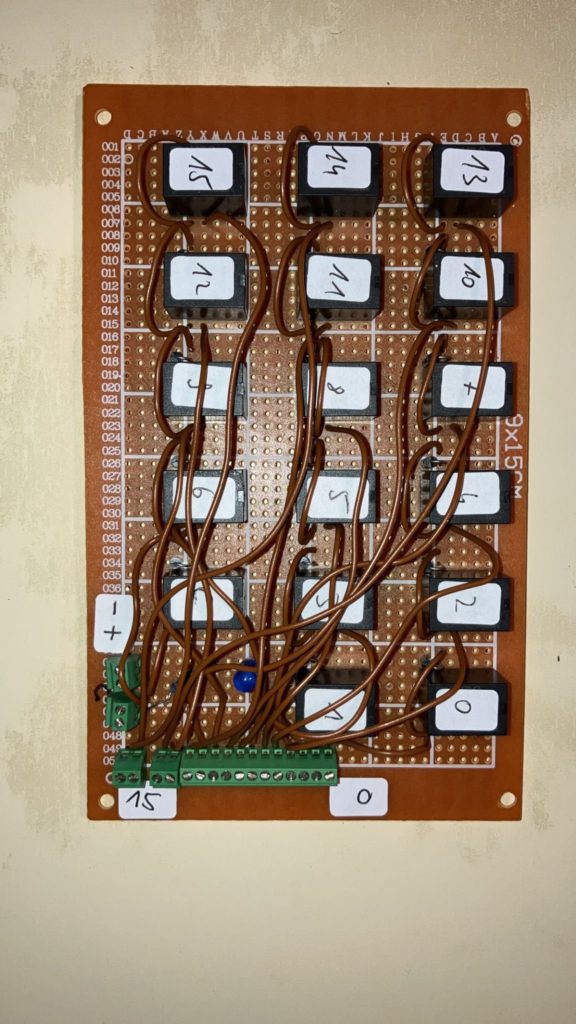
6 days ago • 0 commentsSo, here you see the complete ALU result register. It is a 16 bit register. The board with the 17 black relays is the storage board, 16 relays to store the 16 bits (the relays are holding themself active when switched on), one relay to switch off VCC to clear all 16 storage relays. The two other boards are used as an input enable board from the ALU or as an output enable board to the databus...
![]()
-
Finished the first part of the ALU result register
05/11/2024 at 19:41 • 0 commentsSo, the following little module is able to store a 16 bit value...and will be used as the ALU result register. Two little boards will be next, one as input enable into this register, one as output enable from this register to the data bus.
![]()
You see 17 relays for 16 bit...thats because one relay is used to switch out the 24V to clear the register, this is done by a "Clear" input signal.
-
Finished the first of 3 plates...
05/06/2024 at 14:14 • 0 commentsSo, what you see here is the complete adress-module of the relay CPU...the first of three plates is now complete:
![]()
This module is able to hold a 10 bit program-counter, add +1 if necessary, read/write the program-counter to/from the databus, load a adress from the databus into a adress-register and write the program-counter or the adress-register into an adressbus-register...which is connected to the adressbus.
In the following picture you see the interface:
![]()
-
Finished a new register...
05/05/2024 at 19:57 • 0 commentsThe following picture shows a new 10 bit register for the adress-module. This register holds the adress if a command wants to access the memory, for example LDA M(X),,,Load the accu with the value stored in adress X. This new register holds the adress, a multiplexer is then switching between the program counter or this new register to copy one of them to the adressbus-register. Thats the way the memory is accessed.
![]()
The register was finished in one day and is tested...so the next days I will integrate it into the adress-module.
-
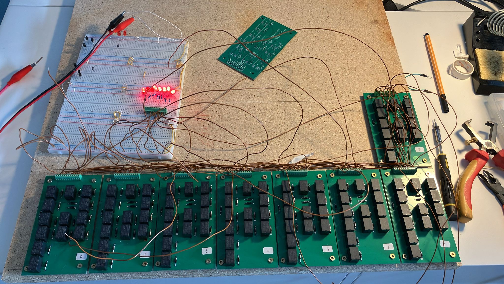
Tested a 8 bit ALU
05/01/2024 at 15:34 • 0 commentsSo, I connected the first 8 ALU boards to implement a 8-bit ALU and tested it. The Shift Left/Right, AND, OR and NOT commands worked perfect. And in the following two pictures you see the calculation of 0x7F + 0x21 = 0xA0 (or: 127 + 33 = 160).
![]()
The first picture shows 0x7F + 0x20 = 0x9F (1001 1111, you see the red LEDs).
![]()
The second picture shows you 0x7F + 0x21 = 0xA0 (1010 0000).
How fast the calculation realy is will be shown in a video, I plan to finish the 16 bit ALU and measure (and documend) the calculation speed of the 16 bit ALU. I need the calculation time to be able to choose a clock timing for clock 1 of the relay system.
-
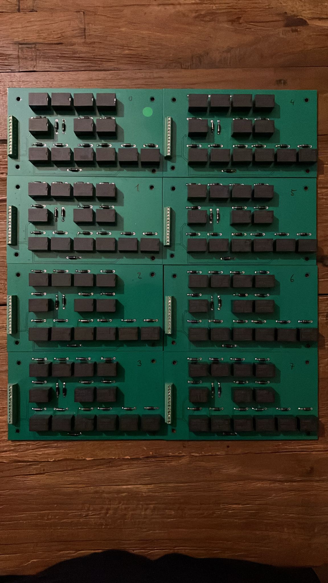
Finished the first 8 1-bit ALU boards
04/22/2024 at 04:36 • 0 commentsThe first 8 ALU boards are finished, during the next days I will mount them together to a 8-bit ALU and test it. Two 8-bit ALUs are then mounted together to the 16-bit ALU used in the system.
![]()
-
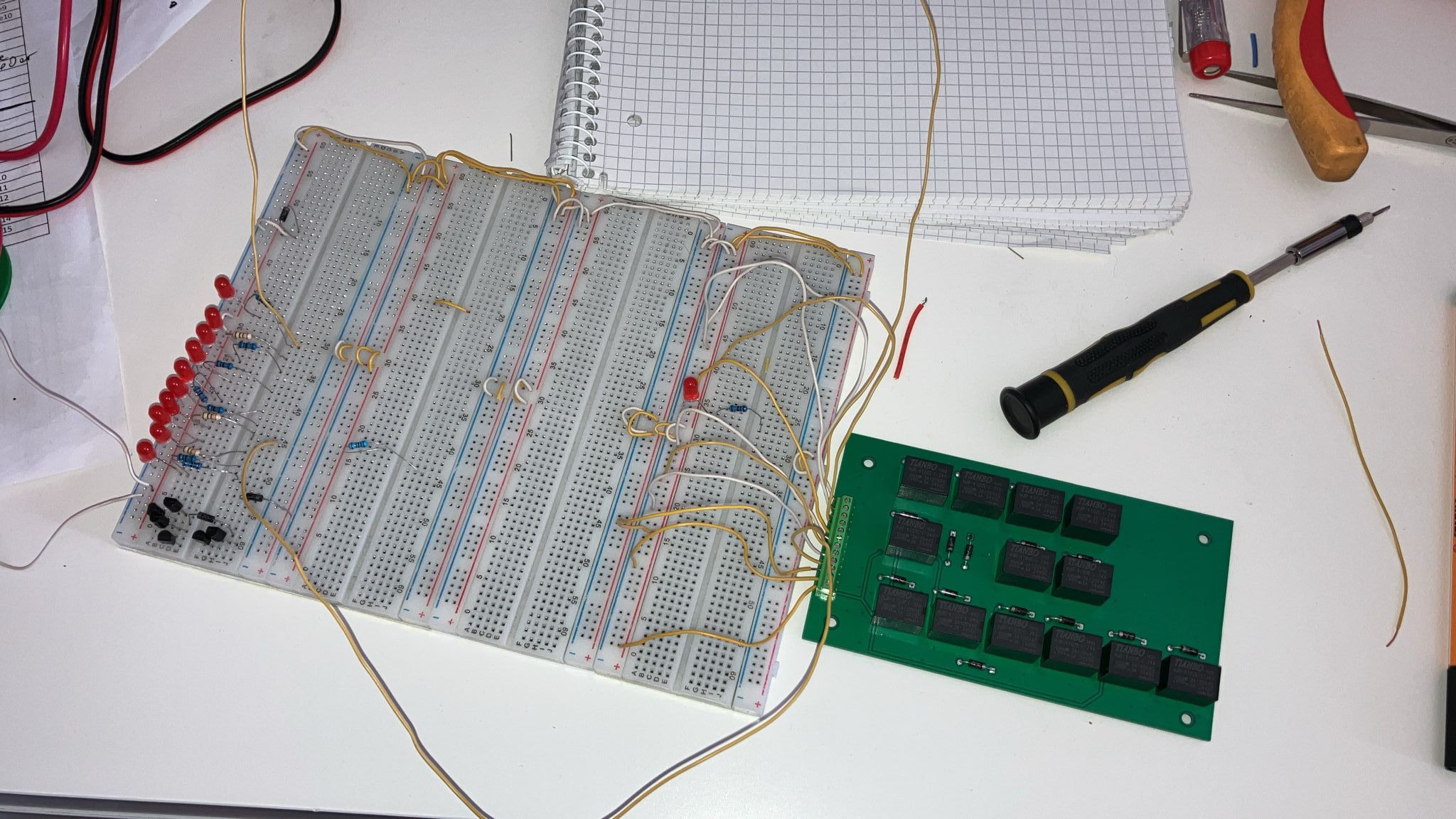
Build and tested the first ALU bit...
04/14/2024 at 08:11 • 0 commentsSo, the first ALU board is build and tested...and it is working! Now I will start building the remaining 15 boards.
![]()
-
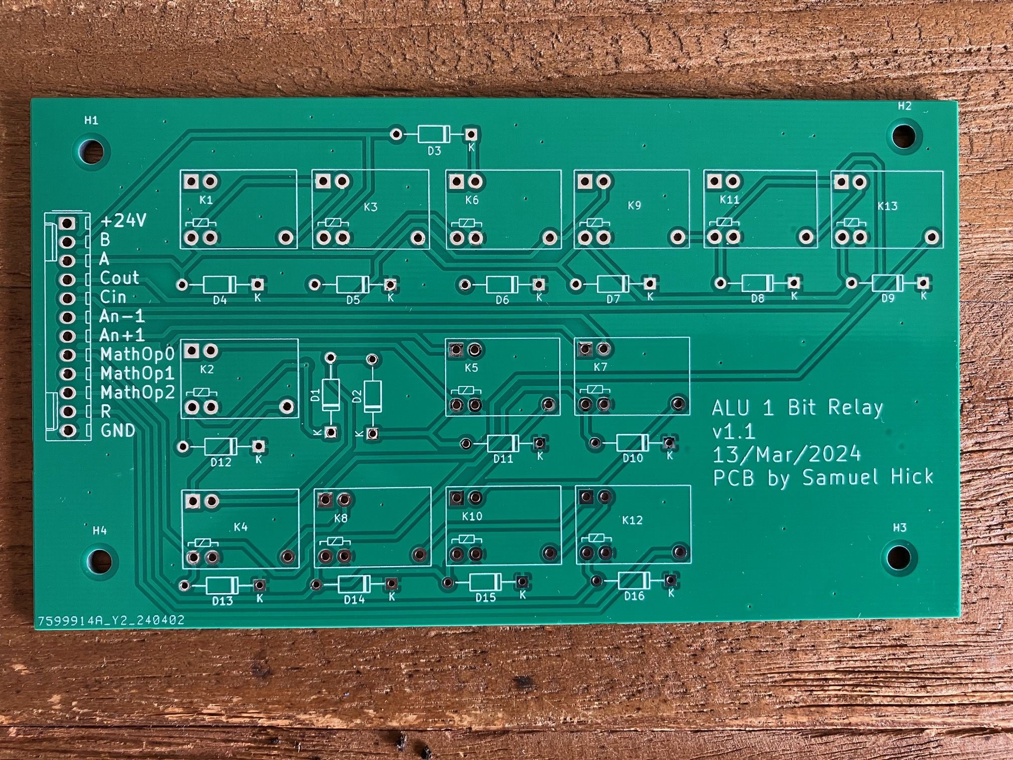
ALU PCB finished!
04/09/2024 at 13:27 • 0 commentsFor the system I need a circuit with 13 relays for each bit of the ALU...16 times the same circuit! Building this connection by connection wouldn't be a very enjoyable task. So, a friendly colleague offered me to design a PCB out of my circuit diagram. I am truly very grateful to him for it.
And this is the result. It only took 1 week from the purchase order to the delivery:
![]()
-
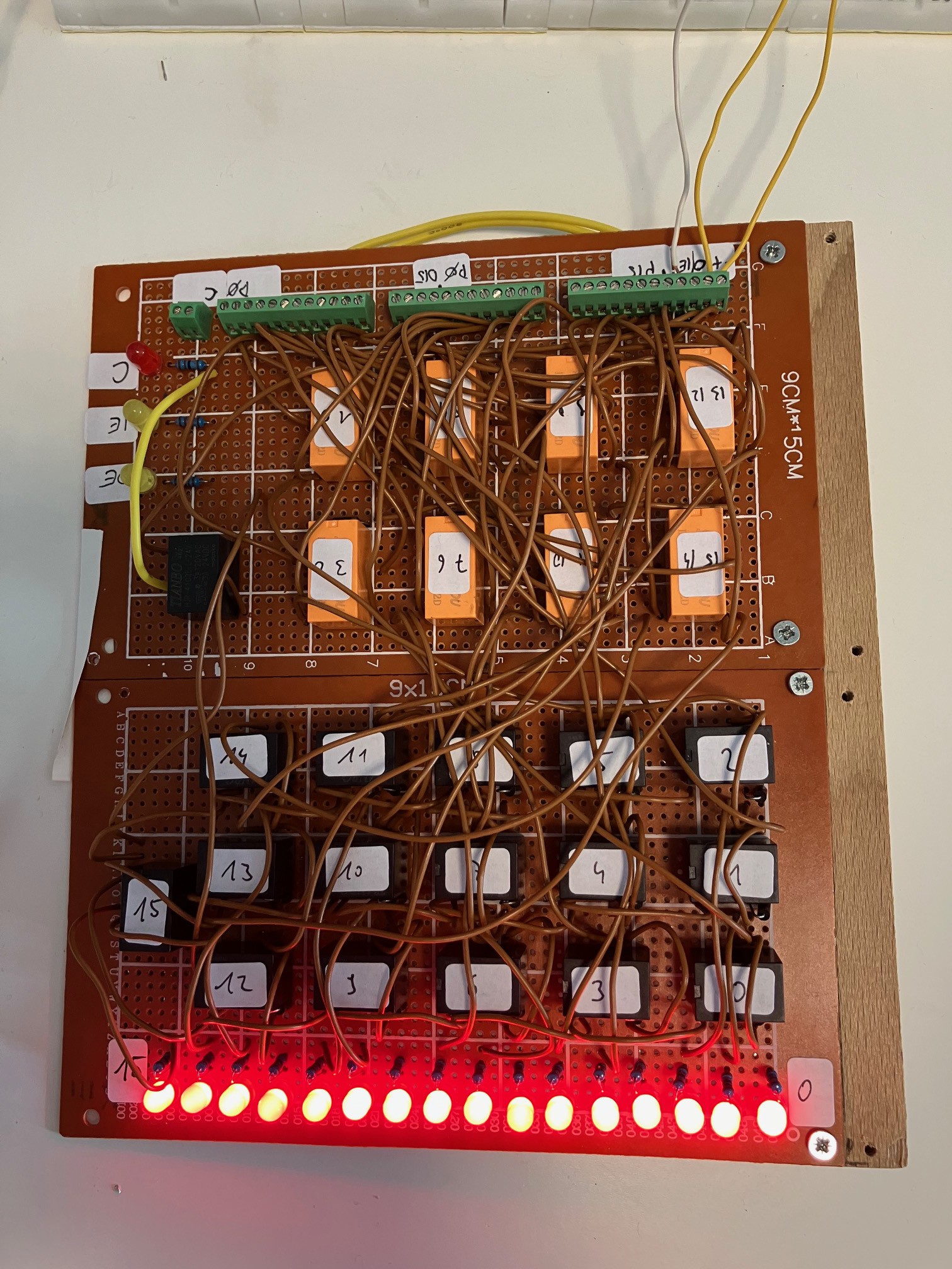
Finished the accumulator register
04/09/2024 at 13:10 • 0 commentsSo, the 16 bit accumulator register, which the register for all mathematical, all store and all load operations, is finished and tested. The next step is to connect the register to the system...
![]()
The 16 black relays with numbers are responsible for storing the bit values (by holding themself in an active state), the black relay without a number releases the VCC (for clearing the stored value) and the orange relays are responsible for Input and Output to/from the databus.
-
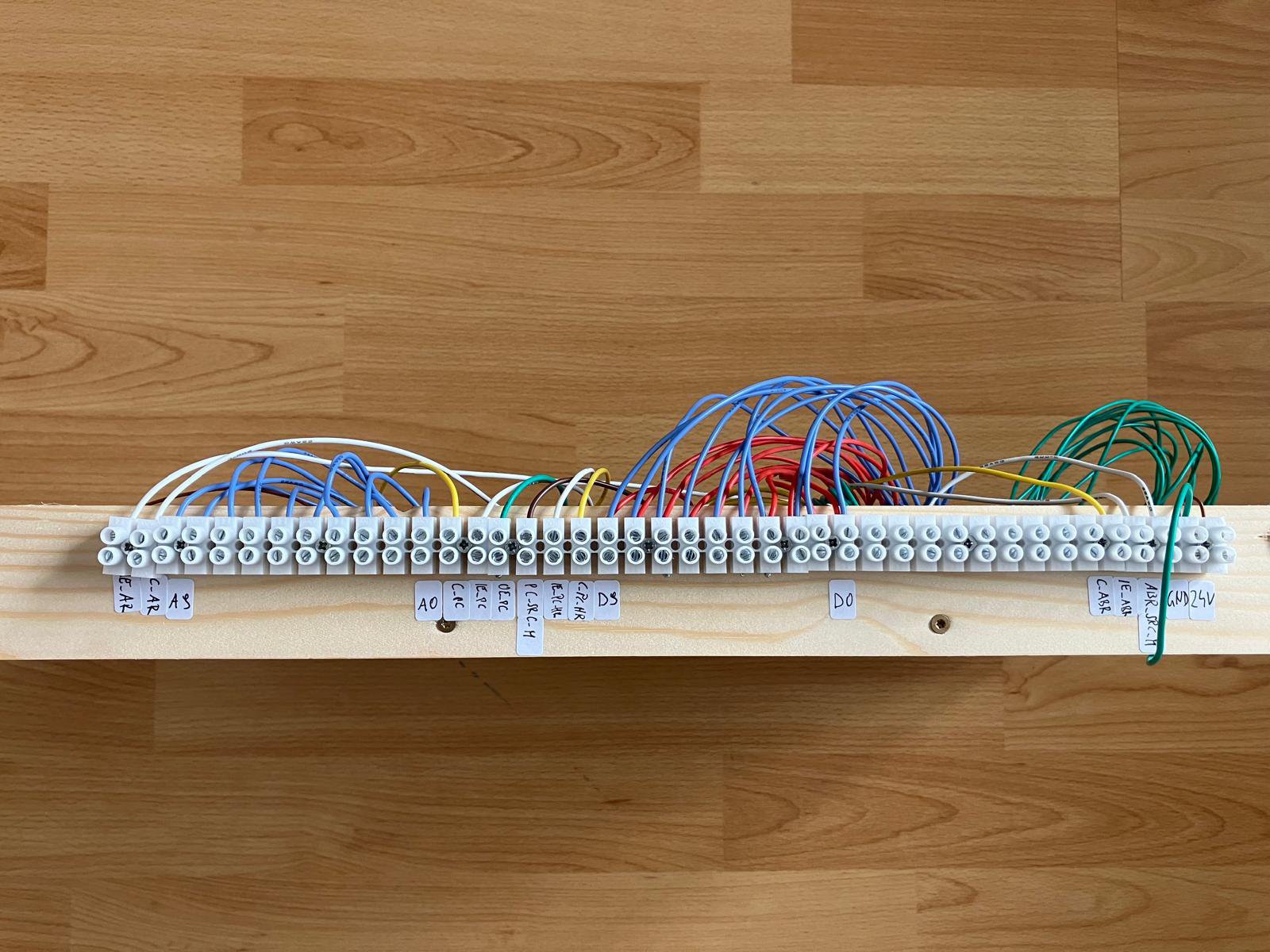
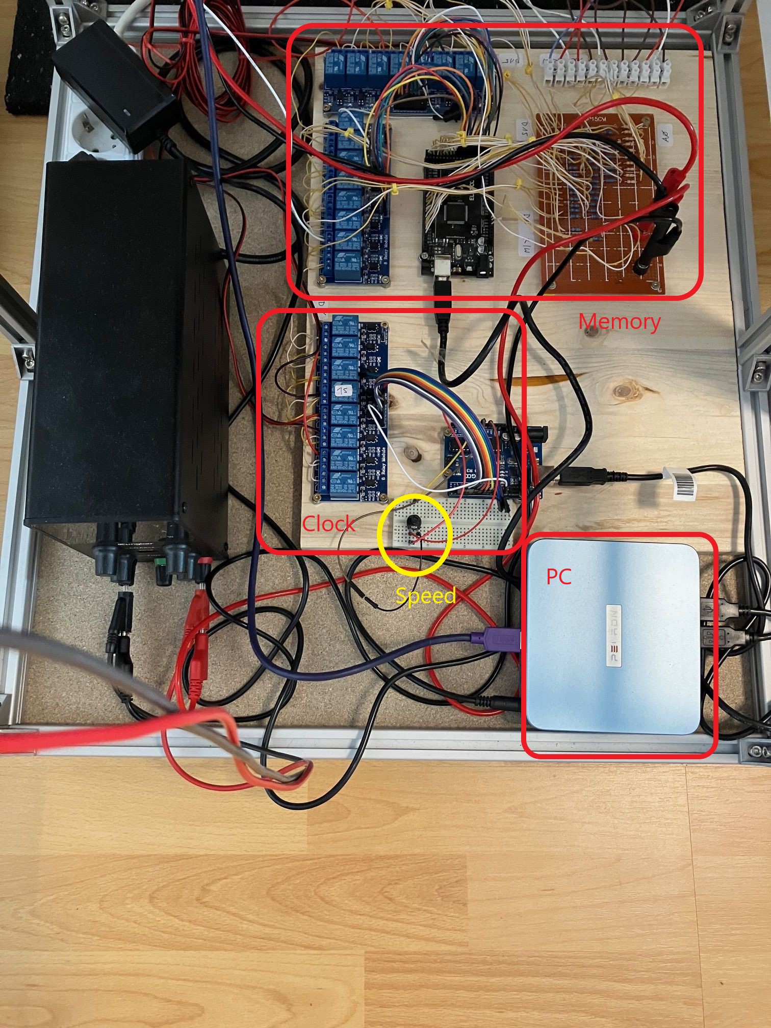
Added a little communication PC
04/09/2024 at 12:46 • 0 commentsSo, I recently added a little PC just for communication, connected to the arduinos and the logic analyzer. And reachable via remote desktop. The following picture shows you the bottom of the system:
![]()
There you see the memory, the new communication PC and the clock. The yellow marked part is a poti connected to the arduino which is responsible for the clock generation to change the speed of the system.
Homebrew 16 bit relay computer
Goal of the project is to develop and build a homebrew 16 bit relay computer