The idea for this design was born at the end of januari (2023).
While many homebuilt CPU's have their own, unique instruction set, I decided that for this project the CPU would use an existing instruction set. Also, I wanted to build the computer from parts of the TTL family. That are integrated circuits, that can perform elementary logic functions. They were first used in the 60's of the previous age. I use a modern version of these circuits, that use less power.
So which instruction set to use ? The CPU inside your laptop or cellphone is much, much too complex to build. But it is possible to use an older CPU from the time when microprocessors just became available. There were two processors that can be regarded as the Beetle and the Deux Cheveaux of the beginning of the homecomputer age.
Those processors are the MOS Technology 6502 and the Zilog Z80.
The 6502 is famous because it was the heart of the Apple 1, the Apple ] [, the Commodore 64, the Nintendo NES and many others. The Z80 is well known because it was used in the TRS-80 and the ZX Spectrum.
So now, I had to decide whether to use the instruction set of the 6502 or that of the Z80. But then I thought... why not build a CPU that can do both ?
I did spend a few months searching for a good design that would give good performance while not using too many parts. I think the basic design is stable now (end of march 2023). I can now start with the details of the design.
BUILD A COMPUTER
A CPU is a nice thing, but on it's own it does nothing. It needs memory, power, and input and output devices. So I planned to build a full computer. Here are the specifications:
Specifications:
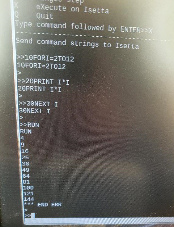
- runs 6502 programs
- runs Z80 / 8080 programs
- processor speed 12.5 MHz
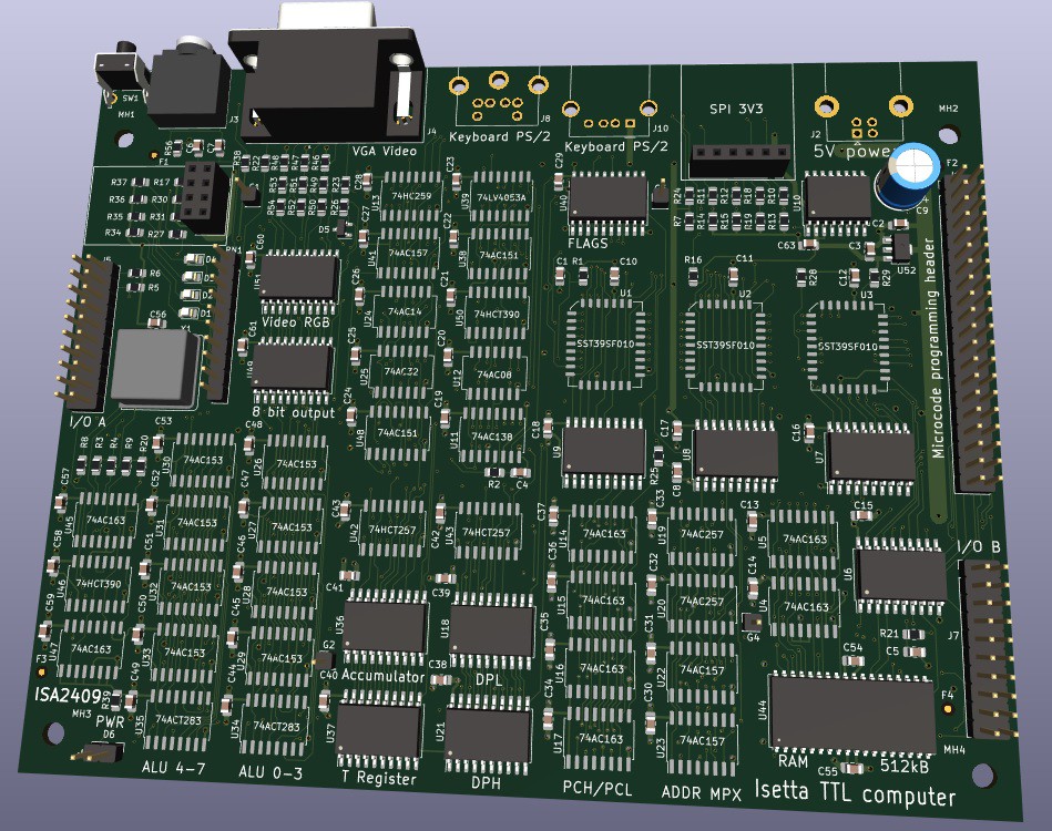
- 512 kByte RAM ( 8 bit wide )
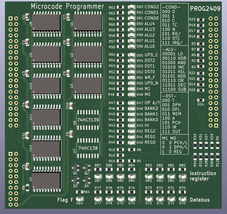
- 24 bits wide microcode in 3 flash chips
- programmable (upgradable) microcode
- On-board SSD 32 Mbyte
- video VGA 320 x 200 pixels, 64 colors
- video VGA 640 x 480 pixels, 64 colors
- PS/2 keyboard connection
- Connection for ESP-01S WiFi card
- Connection for SPI device (micro SD card)
- real-time clock synchronized by WiFi
- sound generator
- blinkenlights (4)
- general purpose I/O
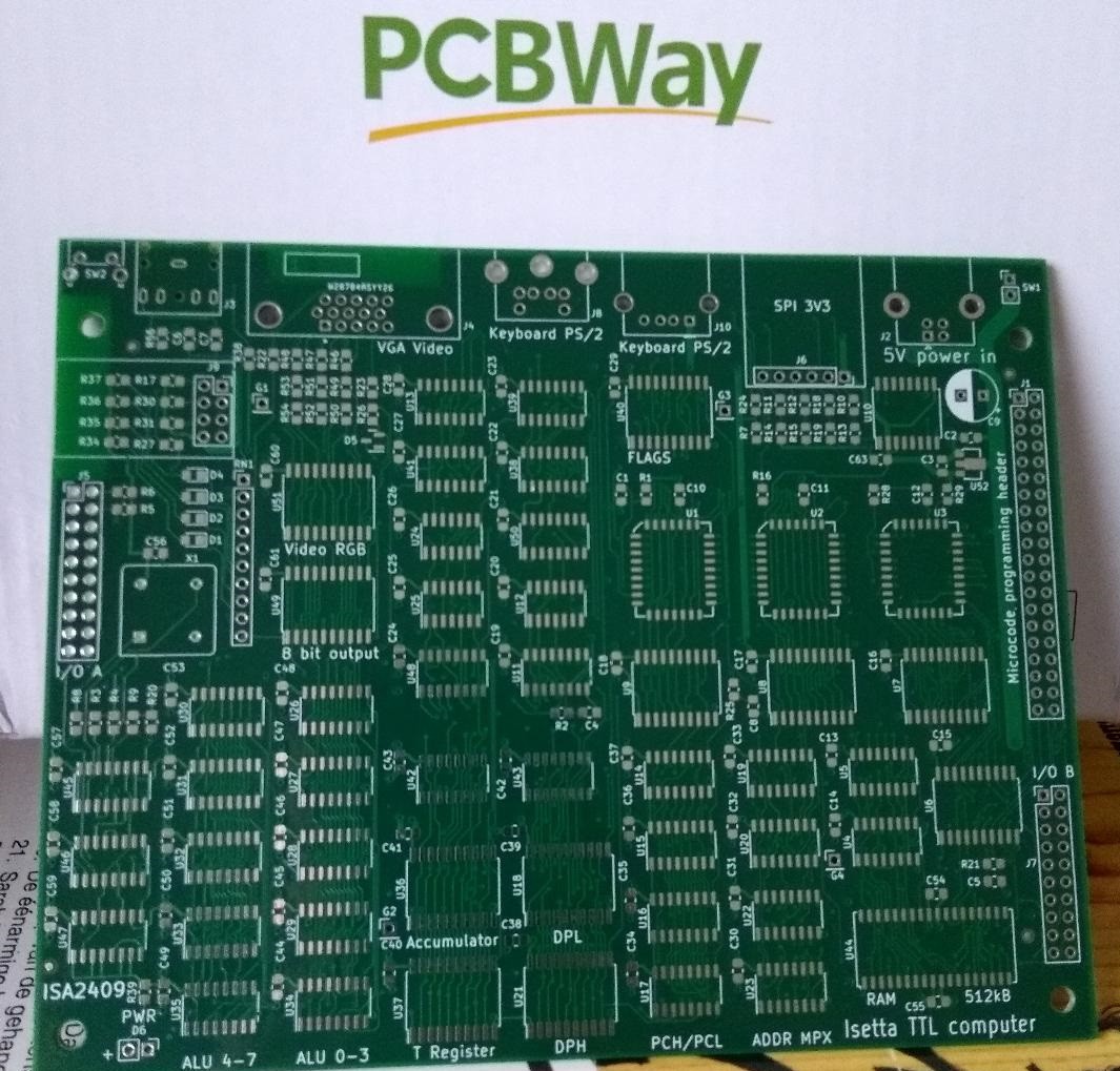
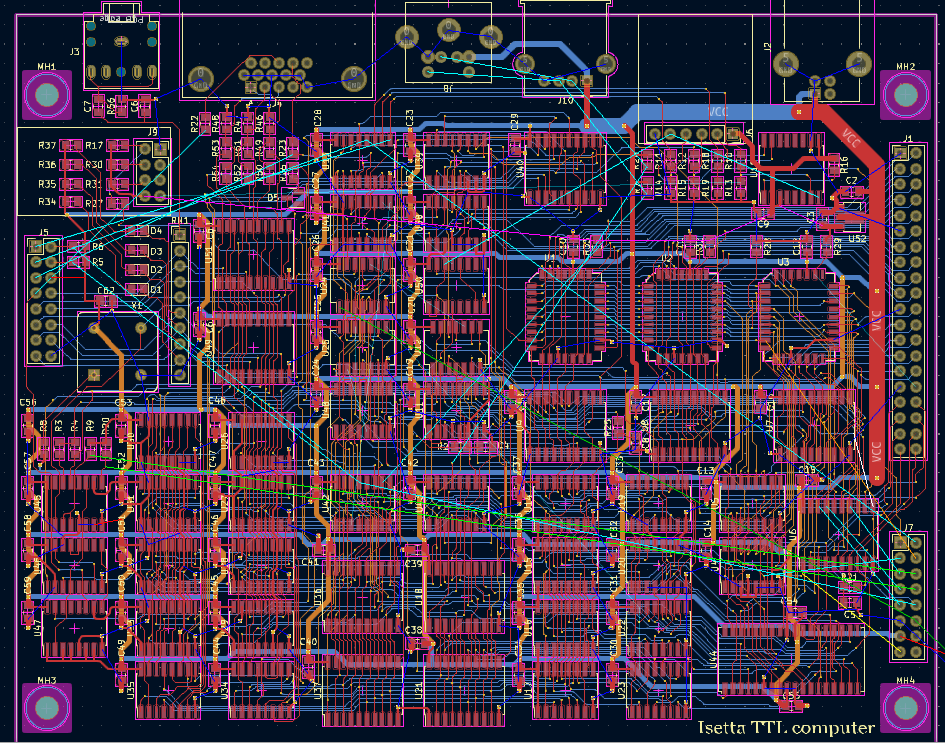
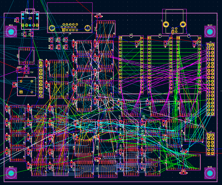
- pcb 119 x 150 mm (4.7 x 5.9 inch), 4 layers.
- powered by 5 volt USB input
Components:
- RAM memory chip
- Three Flash memory chips
- SPI Flash memory chip for mass storage
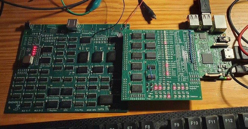
- 46 TTL logic chips (38 CPU, 8 Video and I/O)
Principles for the design:
- No microprocessor, microcontroller, SOC, FPGA, CPLD, GAL, PAL or 74181
- All components have good availability at the big distributors
- Low number of components
- No fine-pitch devices that are difficult to solder
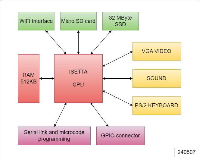
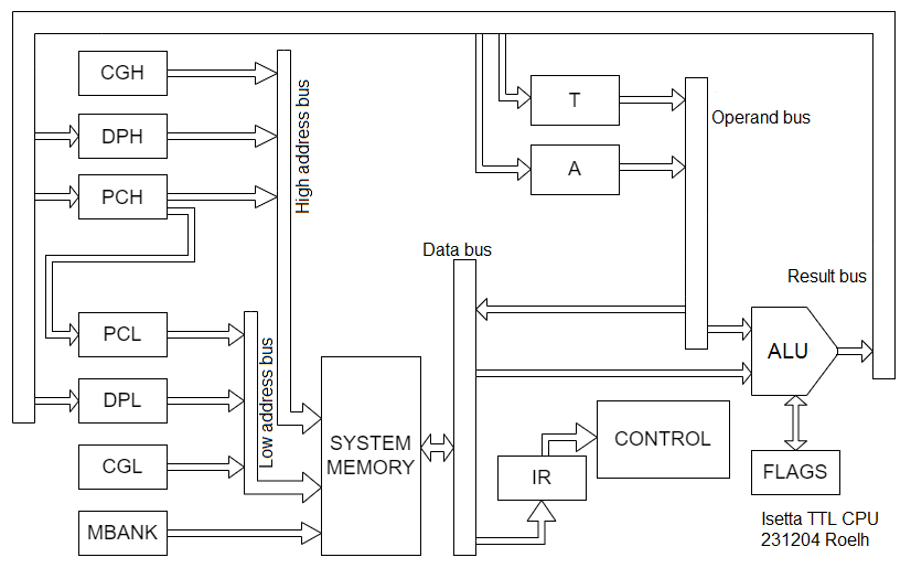
ISETTA SYSTEM DIAGRAM
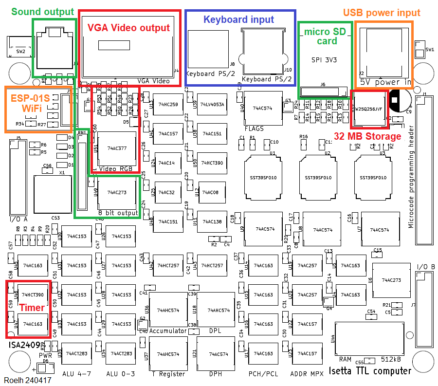
COMPUTER I/O LAYOUT
CPU TECHNICAL DESCRIPTION
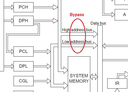
Here comes the system diagram of the CPU. Most arrows and buses represent 8 wires, that means that the information flows through the processor in units of 8 bits (a Byte).
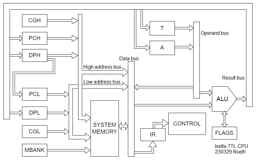
I might as well start with explaining some of the parts.
- PCH/PCL (program counter high byte and low byte)
- A (Accumulator)
- T (Temporary register)
- DPH/DPL (Data pointer high byte and low byte)
- IR (Instruction register)
- CGH Constant generator, generates only 0 (mainly for zpage addressing)
- CGL Constant generator for small integer values
- MBANK Bank selection system
You will miss the 6502 registers S (stack pointer) and the index registers X and Y. And you will miss the long list of registers that are inside a Z80 CPU. Those registers are in memory. A special memory section (outside the normal 64K range) is used for the registers.
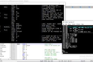
The control section will use microcode to run the whole show. The microcode has 16 pages, 1 page is needed for the 6502 and 5 will be needed for the Z80, and the software can switch between 6502 and Z80. The microcode has room for one or two...
Read more »

 zpekic
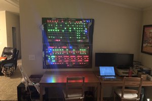
 spudfishScott
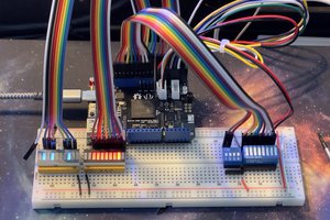
 Tom
Tom
Just been reading your square inch TTL CPU - great work. Did you publish your microcode, or is that proprietary ? Curious how you managed such a rich ISA with so few control signals!