Close
0%
0%

Programming the DE0 Nano for the first time.

'Hello World' for the DE0 Nano.

Similar projects worth following
A simple circuit for an intro to the Altera Cyclone IV on the DE0 Nano.

So, the first first lab in the class that deals with drawing circuits is a couple of XOR circuits, but that is as good a place to start as any.

The circuits:

XOR 1

XOR 2

Using Digital Works Lab

The Logic:

XOR 1
AB
¬A¬B
A∧¬B¬A∧B
(A∧¬B)∨(¬A∧B)
1100000
1001101
0110011
0011000
XOR 2
AB
¬A¬B
¬A∨¬BA∨B
(¬A∨¬B)∧(A∨B)
1100010
1001111
0110111
0011100

The Simulation:

TKGate

Digital Works

*TKGate is definitely not a perfect program. I tested it on one computer, and it ran so slowly that it was essentially unusable, and on another system it seemed to work well, but it would occasionally crash. So regardless of the software being used save early and save often. I was also able to use Digital Works on ubuntu running it under wine.

For me designing the circuits in these simulators was a great place to start.

.......................................................................................................................................................................

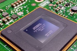
Programming the DE0 Nano:

Here I will detail the steps that I took in order to program the DE0 Nano with the XOR circuits. Because DE0 Nano development board only has two buttons I tied the circuits together, and also keep in mind that the logic is inversed because the switches are normally high and go low when pushed (double check and re-verify this).

Below is the circuit that the fpga will be programmed with.

A pinout with names correlating to the DE0 Nano Documentation and an example qsf file can be found in the project logs.

Ubuntu Step 1) Make sure that the USB-Blaster is working.

Step 2) Create Project

Step 3) Make the Pin Assignments and Draw the Cirucit

Step 4) Handle a compilation error.

Step 5) Program the DE0 Nano.

This simple example will only load the program to the FPGA, and will run so long as power is not cycled. If power is cycled the default program from the EPCS will be loaded.

  • 1 × DE0 Nano Educational FPGA
  • 1 × Linux PC with TKGate or Windows PC with Digital Works
  • 1 × Quartus II Web Edition

  • Some Global Settings & IO Standard

    jlbrian710/07/2015 at 23:06 0 comments

    Globals
    FAMILY"Cyclone IV E"
    DEVICE EP4CE22F17C6
    DEVICE_FILTER_PACKAGEFBGA
    DEVICE_FILTER_PIN_COUNT256


    Other
    IO_STANDARD"3.3-V LVTTL"*This should be the setting for all pins

  • GPIO0

    jlbrian710/07/2015 at 22:28 0 comments

    Here the pin name is prefixed with the letter 'a', but this can be changed to anything unique.

    GPIO0
    PinName
    PIN_A8a_IN[0]
    PIN_D3a[0]
    PIN_B8a_IN[1]
    PIN_C3a[1]
    PIN_A2a[2]
    PIN_A3a[3]
    PIN_B3a[4]
    PIN_B4a[5]
    PIN_A4a[6]
    PIN_B5a[7]
    PIN_A5a[8]
    PIN_D5a[9]
    PIN_B6a[10]
    PIN_A6a[11]
    PIN_B7a[12]
    PIN_D6a[13]
    PIN_A7a[14]
    PIN_C6a[15]
    PIN_C8a[16]
    PIN_E6a[17]
    PIN_E7a[18]
    PIN_D8a[19]
    PIN_E8a[20]
    PIN_F8a[21]
    PIN_F9a[22]
    PIN_E9a[23]
    PIN_C9a[24]
    PIN_D9a[25]
    PIN_E11a[26]
    PIN_E10a[27]
    PIN_C11a[28]
    PIN_B11a[29]
    PIN_A12a[30]
    PIN_D11a[31]
    PIN_D12a[32]
    PIN_B12a[33]

  • GPIO1

    jlbrian710/07/2015 at 22:21 0 comments

    Here the pin name is prefixed with the letter 'b', but this can be changed to anything unique.

    GPIO1
    PinName
    PIN_T9b_IN[0]
    PIN_F13b[0]
    PIN_R9b_IN[1]
    PIN_T15b[1]
    PIN_T14b[2]
    PIN_T13b[3]
    PIN_R13b[4]
    PIN_T12b[5]
    PIN_R12b[6]
    PIN_T11b[7]
    PIN_T10b[8]
    PIN_R11b[9]
    PIN_P11b[10]
    PIN_R10b[11]
    PIN_N12b[12]
    PIN_P9b[13]
    PIN_N9b[14]
    PIN_N11b[15]
    PIN_L16b[16]
    PIN_K16b[17]
    PIN_R16b[18]
    PIN_L15b[19]
    PIN_P15b[20]
    PIN_P16b[21]
    PIN_R14b[22]
    PIN_N16b[23]
    PIN_N15b[24]
    PIN_P14b[25]
    PIN_L14b[26]
    PIN_N14b[27]
    PIN_M10b[28]
    PIN_L13b[29]
    PIN_J16b[30]
    PIN_K15b[31]
    PIN_J13b[32]
    PIN_J14b[33]

  • 2x13 GPIO Header

    jlbrian710/07/2015 at 22:07 0 comments

    (Better map, this is wierd.)

    2x13 GPIO Header
    PinName
    PIN_A14GPIO_2[0]
    PIN_B16GPIO_2[1]
    PIN_C14GPIO_2[2]
    PIN_C16GPIO_2[3]
    PIN_C15GPIO_2[4]
    PIN_D16GPIO_2[5]
    PIN_D15GPIO_2[6]
    PIN_D14GPIO_2[7]
    PIN_F15GPIO_2[8]
    PIN_F16GPIO_2[9]
    PIN_F14GPIO_2[10]
    PIN_G16GPIO_2[11]
    PIN_G15GPIO_2[12]
    PIN_E15GPIO_2_IN[0]
    PIN_E16GPIO_2_IN[1]
    PIN_M16GPIO_2_IN[2]

  • SDRAM

    jlbrian710/07/2015 at 21:51 0 comments

    Here the outline for the SDRAM is barely visible, the chip is on the underside of the board.

    SDRAM
    PinName
    PIN_M7DRAM_BA[0]
    PIN_M6DRAM_BA[1]
    PIN_R6DRAM_DQM[0]
    PIN_T5DRAM_DQM[1]
    PIN_L2DRAM_RAS_N
    PIN_L1DRAM_CAS_N
    PIN_L7DRAM_CKE
    PIN_R4DRAM_CLK
    PIN_C2DRAM_WE_N
    PIN_P6DRAM_CS_N
    PIN_G2DRAM_DQ[0]
    PIN_G1DRAM_DQ[1]
    PIN_L8DRAM_DQ[2]
    PIN_K5DRAM_DQ[3]
    PIN_K2DRAM_DQ[4]
    PIN_J2DRAM_DQ[5]
    PIN_J1DRAM_DQ[6]
    PIN_R7DRAM_DQ[7]
    PIN_T4DRAM_DQ[8]
    PIN_T2DRAM_DQ[9]
    PIN_T3DRAM_DQ[10]
    PIN_R3DRAM_DQ[11]
    PIN_R5DRAM_DQ[12]
    PIN_P3DRAM_DQ[13]
    PIN_N3DRAM_DQ[14]
    PIN_K1DRAM_DQ[15]
    PIN_P2DRAM_ADDR[0]
    PIN_N5DRAM_ADDR[1]
    PIN_N6DRAM_ADDR[2]
    PIN_M8DRAM_ADDR[3]
    PIN_P8DRAM_ADDR[4]
    PIN_T7DRAM_ADDR[5]
    PIN_N8DRAM_ADDR[6]
    PIN_T6DRAM_ADDR[7]
    PIN_R1DRAM_ADDR[8]
    PIN_P1DRAM_ADDR[9]
    PIN_N2DRAM_ADDR[10]
    PIN_N1DRAM_ADDR[11]
    PIN_L4DRAM_ADDR[12]

  • EPCS

    jlbrian710/07/2015 at 21:37 0 comments

    EPCS
    PinName
    PIN_H2EPCS_DATA0
    PIN_H1EPCS_DCLK
    PIN_D2EPCS_NCSO
    PIN_C1EPCS_ASDO

  • Accelerometer & EEPROM

    jlbrian710/07/2015 at 21:33 0 comments

    (Why are these tied together? Implications?)

    Accelerometer & EEPROM
    PinName
    PIN_F2I2C_SCLK
    PIN_F1I2C_SDAT
    PIN_G5G_SENSOR_CS_N
    PIN_M2G_SENSOR_INT

  • ADC

    jlbrian710/07/2015 at 21:26 0 comments

    ADC
    PinName
    PIN_A10ADC_CS_N
    PIN_B10ADC_SADDR
    PIN_B14ADC_SCLK
    PIN_A9ADC_SDAT

  • Switch

    jlbrian710/07/2015 at 21:24 0 comments

    Switch (DIP Switch)
    PinName
    PIN_M1SW[0]
    PIN_T8SW[1]
    PIN_B9SW[2]
    PIN_M15SW[3]

  • Key's

    jlbrian710/07/2015 at 21:21 0 comments

    Key (Push Button)
    PinName
    PIN_J15KEY[0]
    PIN_E1KEY[1]

View all 13 project logs

Enjoy this project?

Share

Discussions

Brian K. White wrote 11/08/2021 at 00:03 point

Nice load of dead links

  Are you sure? yes | no

Similar Projects

Does this project spark your interest?

Become a member to follow this project and never miss any updates