PK
PK-
What Gives?
08/12/2014 at 03:00 • 0 commentsSorry for the info dump the other day; I didn't have time to write up something real.
But, seriously, PCBs were ordered - why be mad? Let's start with pictures of my reference design, and talk about what I added, what I could/should have done better, and why I made some choices.
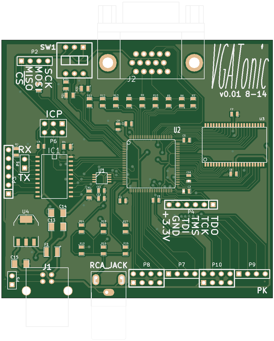
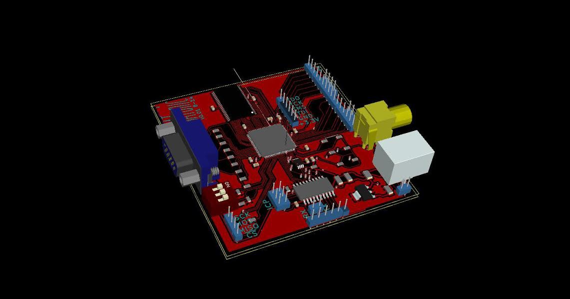
But first, a picture of the top of the PCB and a render, of course!
![]()
PCB Top with Silkscreen
![]()
Rendering of VGAtonic from Kicad
So, What's New?
Tons... at least compared to the working demo. You'll note that we've added the XC95144XL now, and I'll stop playing with the 64 and 72 macrocell poseurs. We've added the memory I discussed two posts ago, the ISSI IS61LV5128AL-10. I've added an LTC6903 programmable oscillator to play with the clock, and, because it's almost always a good idea, I added a microcontroller (AVR ATTiny 2313a) with a few extra lines routed to the CPLD for whatever fun features we dream up.
I also, of course, made a basic power supply. Power comes in through the USB-B jack, goes through a PTC, then into a basic 3.3v regulator, ON Semiconductor's NCP1117ST33T3G.
For decap, I just used X5R .1uF capacitors near the power pins, all on the topside for ease of assembly. The '6903 got an extra 1uF capacitor too, for good luck. There are a couple others near the power supply (2x 10uF and a 47uF) - see my schematic in the git repo for details.
So, What Could Be Better?
Well, for one, I had no size in mind - I want it to roughly fit in a 4x6 picture frame, *maybe*, so I ended up with 3"x3". I think it might make more sense to aim for something real - I've heard some rumblings of DIP compatible, so maybe a future version should "barely fit on a breadboard". You tell me.
Second, I left vias in some pads - I thought I moved those, but the design doesn't lie. I'm not to worried about my solder bleeding through the holes though because for the passives I'll be hand soldering using leaded paste.
Third, for some reason my VGA footprint doesn't have anything exposed on the backside to solder too. This won't be a huge problem though: just flood it so the solder flows to the other side.
Fourth, (nitpicky) the RCA jack's alignment post hangs off the board. It would be better to have left something for it to stay on.
Fifth, I probably should have done better with that ground plane - but at only 50 MHz, I'm not too worried about it. I'll eat those words if I can't get any output, of course, but for a first draft it'll do.
Why Did You Do _______?
Obviously, I made a few game-time decisions here - adding the programmable oscillator and AVR will help with the prototyping and firmware, and the extra routes from the ATTiny might come in handy for something.
For I/O I had plenty of extra pins. I routed 3 to DIP switches, and I made a Papilio compatible Wing ( http://papilio.cc/ )... so you can add whatever you want to this and use it like a normal CPLD breakout if you want. Or, you know, add 2 more VGA ports to your VGA controller so you can VGA while 2x VGAs.
USB power was because I have a ton of USB-B cables and computers and chargers to plug them into. I suppose I could have used a typical barrel jack, but... it'll be fine (and I didn't want to bother with a 5v regulator).
Also, you'll notice the resistor ladder for VGA grew by one - RRR GGG BB and a third B. We'll use the last B if we want to get true greys and white - so technically, we'll have 512 colors to play with (but everything will be 8 bits wide, so we'll have to make some cuts).
All in all, I'm happy with the first effort - let's get a picture on it now, shall we?
-
Design Files Updated on git
08/10/2014 at 03:02 • 0 commentsI wanted to notify anyone who is interested that I've added design collateral for VGAtonic v0.01 to Github, if you'd like to poke around: https://github.com/dqydj/VGAtonic/tree/master/First_Draft
Gerbers, BOMs and PDFs in schematic form for everyone... and if you use Kicad, you can also find the pcb file and the schematic.
I don't have time to delve into the details now, but expect a further update covering the 'errata' (read: 'warnata') and my regrets with this board. I'll point out the not so great parts too... but this should work just fine as a proof of concept.
-
Yes, But Why?
08/08/2014 at 03:23 • 0 commentsWelcome to all the new followers! The attention is appreciated (and thank you to HaD for the feature) - and it gives me hope that more folks than just us in the PK household will get some use out of this thing.
By day, I'm an engineer - and one of my responsibilities is to write a fair amount of documentation. Of course, it's usually retrospective - here's what we did, here's an application where you can use this.
Hopefully, with this project I can delve a bit more into the "why did you make these decisions?".
That way, even if I can't teach you anything, I can at least reveal my way of thinking... and give you folks ample opportunity to tell me why I'm an idiot.
Why Use an XC95144XL CPLD?
The Practical Reasons
- Cheap
- Hand Solderable (arguably - .5mm pitch is the smallest I've ever hand soldered)
- Easy to Understand
- Well supported
- 5V tolerant
The Personal Reasons
- Already have ISE Webpack on the PC (don't discount this)
- The Challenge™ *
*If you count hardware hacking as a hobby and you don't appreciate the challenge of fitting things into places they shouldn't fit (like display controllers and small CPLDs), you're in this for the wrong reason.
I mean, I've got plenty of working VGA/DVI/HDMI/RCA outputs on equipment here - there's no mandate to improve the PogoPlugs and the Galileo. This is just more interesting to me than watching TV or playing video games available to me because of some other engineer's hard work.
Okay, let's switch gears to the actual update and discuss the strategy with the next challenge - addressing the framebuffer memory. Hopefully this will be very useful to any of you folks deciding how to manage the write cycles in your video projects!
Our target is ISSI's IS61LV5128AL, an 100 MHz 4 Mbit SRAM.
Memory Read/Write Addressing & Timing
There are five approaches to addressing memory quickly in a framebuffer (that I can think of - please add more in the comments!):
- Switching Buffers - Use two memories, when one is complete, switch the read/write memories. Many modern graphics cards use this.
- Blanking - Only update the framebuffer in the horizontal and vertical blanking intervals. Microcontroller VGA/NTSC hacks like to employ this.
- Zero Bus Turnaround - This one is out due to the memory choice, but it's possible to flip instantly between reads/writes on some parts. (Part specific)
- Dual Port RAM - Let the memory handle the collisions - separate read/write ports. (Part specific)
- Interleaving Reads and Writes <- Our choice
This is an easy decision for this project. Because we don't have dual edge flip flops available on the XC95144XL, we're going to use a clock running at two times the pixel clock - so, for VGA, approximating 50.35 MHz. Because of that, we're going to have enough clock events to do this easily. No sweat, in fact - we're going to have about 5ns to spare.
We will have to commit a sin, though - by using the clock in our combinatorial logic (please forgive me!) we can make use of all four edges in the "50.35 MHz divide by 2" pixel clock. Clever or insane, you decide, but here're the critical timing constraints we need to meet (min or max, depending on what is worse):
- Read Time: 10 ns
- Output Enable OFF to High-Z: 4 ns
- Write Cycle Time: 10 ns
- Write Enable Pulse Width (when Output Enable is Off): 8ns
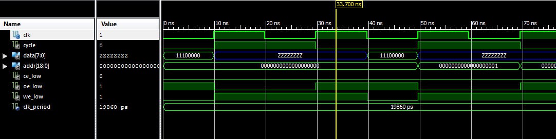
All Wrapped Up in a Neat Little Package
So, I told you we have 4 edges here for each fake-25.175MHz clock, each taking 19.86 ns:
Read and Write cycles require 2 edges, since 19.86/2 < 10ns. This means we need to swap read and write addresses on every rising edge.
When we turn off output enable, it actually takes 4ns before the bus is clear - so we burn an edge, meaning our read cycle is 19.86ns*(3/2).
As luck would have it, we only need to pulse Write Enable for 8ns - which means we'll meet timing requirements with almost 2ns to spare. Here's the pseudocode (where CYCLE can be 1 or 0, dividing our 50.35 MHz clock in two):
Chip_Enable: Always On

Output Enable: On when CYCLE = 0

Write Enable: On when CYCLE = 1 AND CLK = 0

Address: Read Address when OE is on, Write Address when it is off.

Data: On when Write Enable is on, otherwise High-Impedance -- Why?  Because normally the memory will be on the bus.
And here's the timing diagram, ripped out of ISim (ignore the address not changing during the first 2 CYCLEs - in the simulation, both write/read addresses start at 0s). The cursor was placed at the point when the memory will stop writing to the bus - as you can see, we have plenty of time to spare:
![]()
Also note: active low signals.
Closing Thoughts
I'm actually a bit behind on updates - please forgive me, videos are kind of hard to make. The PCBs have been ordered for my version 1 reference design, so I will be adding schematics, gerbers, and KiCad collateral to the Github repo soon (maybe Saturday during the day?): https://github.com/dqydj/VGAtonic
And, yes, I'll be talking about where the PCB was... how do you say... a bit 'suboptimal'. But it'll work - fingers crossed!
-
Proof of Video Life
08/05/2014 at 03:25 • 0 commentsToday's update is one of those "it's really coming together" type updates.
Since you're reading text and you'll probably scroll down anyway, let me blow the surprise: it's VGA and NTSC test patterns. On a 64 macrocell CPLD. From a single, 3.5795454 MHz clock source.
Here's what you'll need to build it:
My code, conveniently located on the Git Repository for VGAtonic and MIT'd for your consumption: https://github.com/dqydj/VGAtonic/tree/master/ColorTest
- 3.5795454 MHz crystal (or a way to get it - 14.318 divided by 4 works)
- A switch (decide on NTSC or VGA mode)
- CPLD/FPGA - note that it needs to allow dual edged flip flops - or you'll have to update the logic to handle 2x the clock. The Coolrunner II XC2C64A in the video allows this.
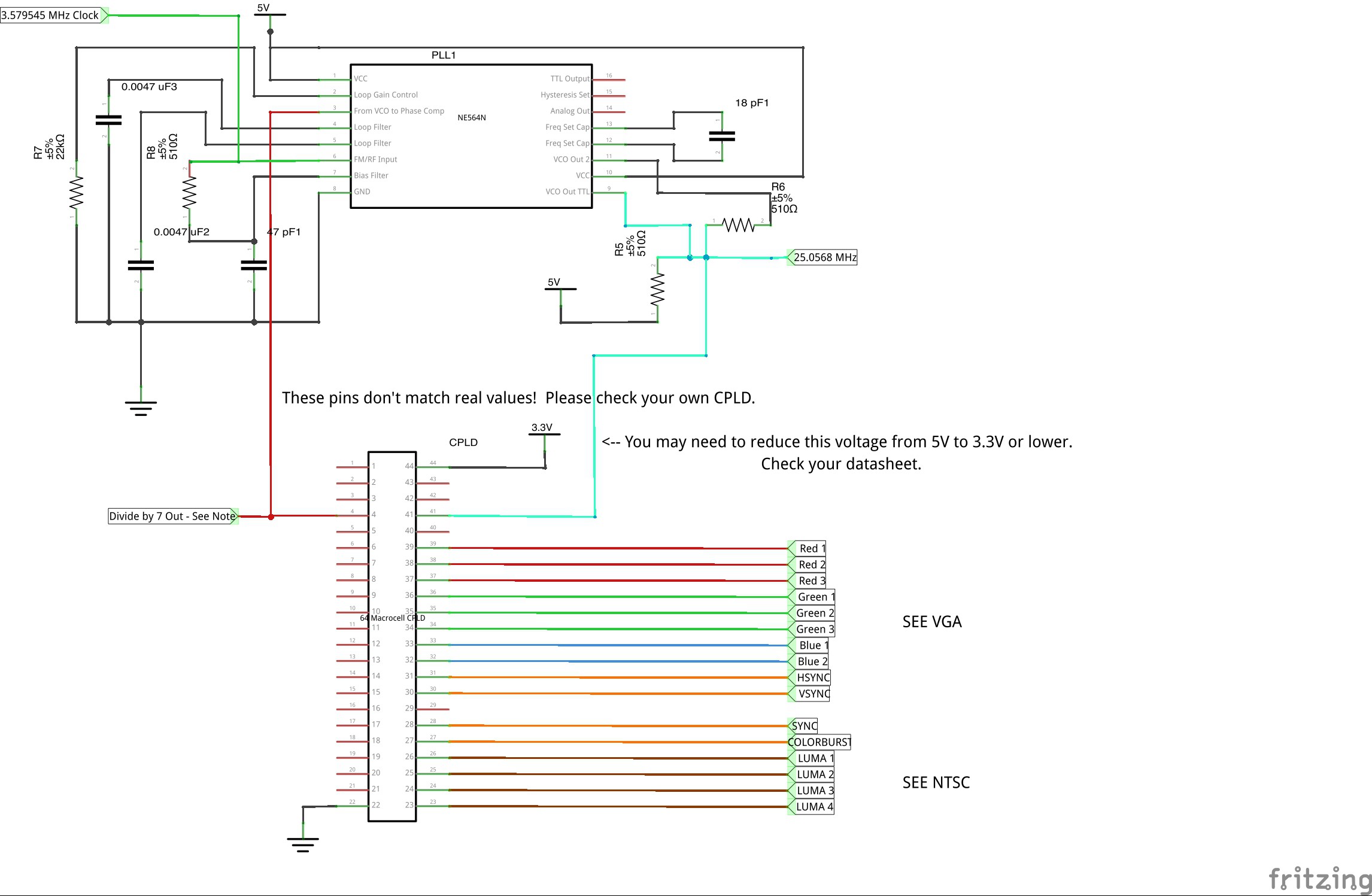
- An NE564 PLL
- 5V Power source, 3.3V regulator, and possibly a way to step down the 5V clock from the PLL (I ignored it, but you shouldn't - it'll likely eventually break the CPLD).
- A bunch of passives to build the resistor ladders and PLL support:
PLL:
- 18 pf Capacitor (I'm using a bunch of 10s and 12s in parallel/series to get close in my image)
- 2x .0047uF Capacitor
- 22k ohm Resistor
- 47 pF Capacitor
- 3x 510 ohm Resistor
VGA:
- 24x 510 ohm Resistor (I use them in parallel to get 255 ohm in my ladder)
- Generic VGA Connector
NTSC:
- 12x 510 ohm Resistor (Again, in parallel to get 255 ohms as well)
- 1k ohm Resistor
- 1.5k ohm Resistor
- Generic RCA plug
![]()
And the NTSC/VGA resistor ladder DAC detail:
![]()
I've got it on a beast of a breadboard - one of those 4 column deals. Here's what it looks like:
![]()
Some notes:
- Separate your grounds with homeruns back to the power supply, if you can. It was easy on my breadboard.
- Use a buffer or a resistor voltage divider or something to knock that clock down to a safe level for your CPLD.
- Add decap to the PLL and the CPLD - you've got long wires and the disgusting parasitics of a breadboard.
Hope someone finds this useful!
I'm sufficiently confident now that VGAtonic is realistic - I'll be designing the PCB next, and I'll throw together the framebuffer code at the same time.
-
Circling Back
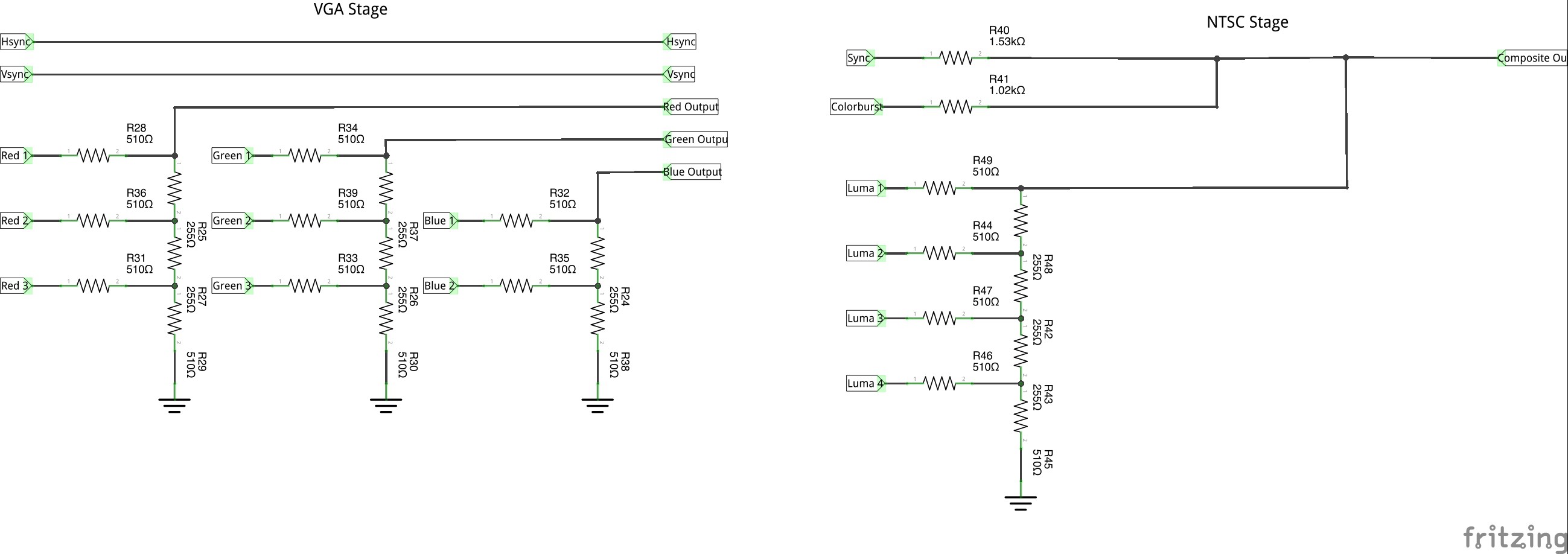
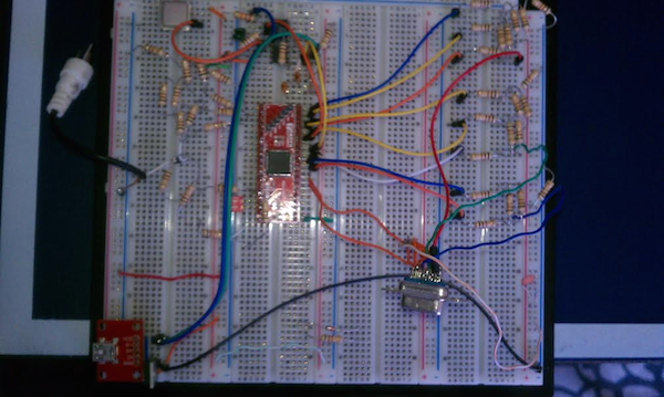
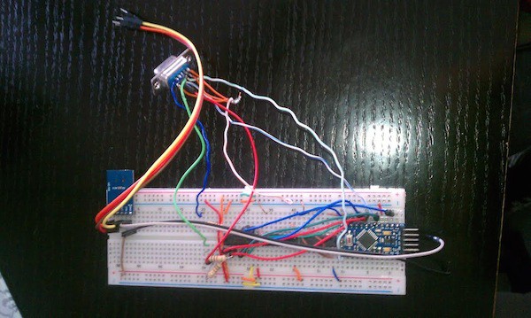
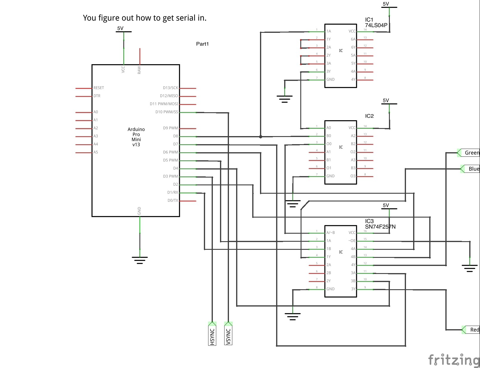
08/03/2014 at 19:29 • 0 commentsOne of my first video projects (other than the hinted-at SPI screens from my introduction video) was getting 640x480 VGA out of an Arduino by addressing 2 pixels per clock cycle. All work and no play makes PK a dull man, so while I was placing a parts order for VGAtonic I ordered a few F-class 74 logic chips to clean up that project a bit - we're down to an Arduino and 3 pieces of external silicon (well, and a temporary serial input if you want to program it from your Arduino IDE).
My original post: http://dqydj.net/how-to-produce-640x480-vga-color-video-from-an-arduino/
Hackaday's coverage: http://hackaday.com/2014/06/10/640x480-vga-on-an-arduino/
The new BOM: 470 ohm resistors for Red/Green/Blue, 68 ohm resistors for Hsync/Vsync plus:
* Some serial input (That's an FTDI breakout in the picture)
* Arduino Pro Mini
* 74LS04P
* 74F86N
* 74F257NHere's how it looks on a breadboard:
![]()
And here's the updated schematic:
![]()
Now, back to your regularly scheduled non-hacky project, VGAtonic - I'll be recording a video with the newest update.
-
Let There Be VGA
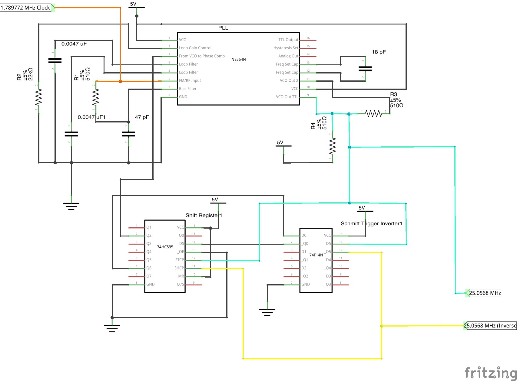
07/31/2014 at 06:43 • 0 commentsQuick one tonight - I wanted to share my setup for generating a VGA-sorta-compatible frequency from a NTSC signal.
No microcontrollers necessary - just a fast inverter, a shift register, and a NE564N PLL on a breadboard (sprinkled with passives).
![]()
The 1.789772 MHz clock is divided down from an NTSC-colorburst compatible frequency - in this case, 14.31818... but you could also use the colorburst signal itself and divide it by 2. The only reason we divide by two up front is to avoid the 'multiply by an odd number' annoyance, since we can't fake it with a non-50% duty cycle with the NE564N. (Many PLLs won't care).
Anyway, this drives all 4 VGA screens in my house.
-
SPI & Clock Domain Crossing (Finally Something Useful)
07/27/2014 at 22:41 • 0 commentsWhen I started looking into doing the input for this project, one of the most common methods of dealing with the multiple clocks in SPI and User Logic land was to... ignore it completely. By using the User clock to sample the changing SPI input signals, you can make a reasonable input stage to whatever you're making.
Of course, that method comes with a large downside, pointed out by Mr. Harry Nyquist (and contemporaries Shannon, Whittaker and Kotelnikov) - your maximum SPI speed is then limited to half of your user clock. That might be fine for many applications, but rate limiting my SPI to 1/2 of the 25.125 MHz clock (12.5625 MHz) might become a major limitation - considering each send of 8 bits is just one pixel!
Here's my take on crossing the clock domain from SPI to user logic, which you can find at my newly published Git repository for VGAtonic:
https://github.com/dqydj/VGAtonic/tree/master/SPI_Demo
I hope you'll check my math, but my take on the maximum speed of this implementation is:
(3*tUSER + 2*tSU)/7.5 ns
For a clock of 25.125 MHz (39.801 ns) and our chosen part the XC95144XL-10 (3.0 ns setup time), I get a maximum speed of 1/16.7204 ns, or 59.807 MHz.
That should cover even the Intel Galileo's SPI, which can run up to 25 MHz.
As for efficiency of flip-flops, here's what we lost in the tradeoff:
* 2 FFs for reset sync in user logic
* 1 FF for reset flag from SPI
* 2 FFs for register full
* 1 FF for register full flag from SPI
* 8 FF for the one-byte FIFO (philosophy: is that still a FIFO?)
* -1 FF, since we only need a 7 bit wide buffer for the SPI domain now.* = 13 extra FFs to cross clock domain
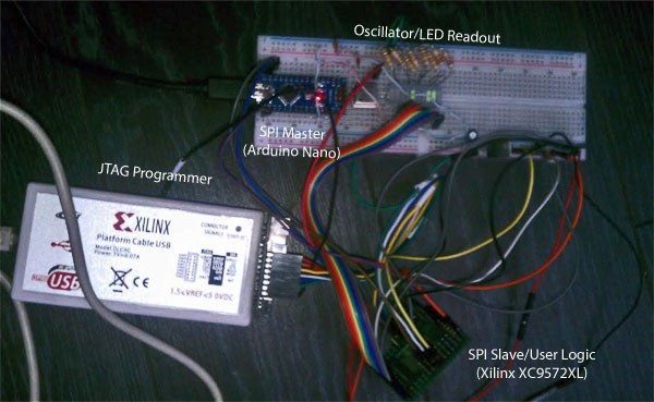
Here's a picture of it working with 1 MHz SPI and a 14.318 MHz user clock on an XC95144XL (LEDs are tied to a register in the user logic domain).
![]()
Hope some of you find the code useful - and please let me know if you can shave off any more FF usage!
-
More Clocks than Flavor Flav
07/27/2014 at 00:20 • 0 commentsWorking on Video isn't particularly hard once you understand the clocks that go into the various technologies, but it's certainly tricky. A perfect example is NTSC video, which has a few "must hit" frequencies:
3.5795454 MHz (literally, 315/88), the colorburst frequency
30 Frames Per Second (literally, 29.970), the vertical refresh rate
15,734 Lines Per Second, the horizontal refresh rate (originally 15,750 in B&W)NTSC encodes color using 'chrominance' - think of a color wheel, where the reference color starts as a yellowish greenish sort of hue, and all the colors of the rainbow are shifted around 360 degrees. Those 360 degrees map to the phase of the clock itself - when you 'paint' a color in NTSC, you really just need to let your 3.5795 MHz reference signal through, phase shifted to represent the actual color you desire.
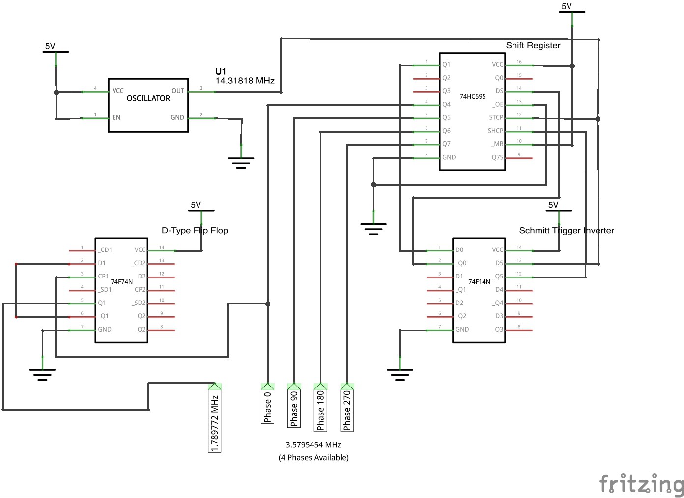
Here's the breadboard circuit I used to get 4 phases of color when first experimenting with NTSC (just sum phases together with a resistor, or delay them using slow digital logic to get even more):
![]()
As an aside (and perhaps as a useful piece of reference for your own video projects) - the phase angle and the horizontal reference rate allow you to determine how accurate your color clock will be if you're somehow synthesizing your color clock and not using a crystal reference. Figure out how many Hz your clock will drift per line, and divide it by 15,750 to find out the maximum color error from the right side to the left side of the screen.
That drift can be exploited to make an NTSC color tester, actually - a 3.595295 MHz crystal will drift exactly 360 degrees out of phase per row, giving the rainbow of the NTSC color gamut. And, more relevant to folks also playing with VGA: a (25.175/7) MHz clock will be off by 16,883 and give you a bit more than a rainbow.
-
You Must Construct Additional Pylons
07/23/2014 at 03:47 • 0 commentsLet's talk about resources - which are far more scarce on our chosen target (the lowly CPLD) compared to its larger cousin the FPGA.
I had a couple Xilinx Coolrunner II CPLDs in my parts bin - I bought them on a whim since they were cheap and interesting (this is the CPLD folks used for that so-called XBox Glitch hack, the xc2c64a). Their stats: 64 macrocells, and 33 I/Os. Well, that won't cut it for our purposes - we need 10 I/Os for VGA @ 8-bit color, 8 I/Os for our memory I/O line and... 19 I/Os for the address.
Not happening. The I/O crunch got us.
So, I bought some 72 Macrocell Xilinx CPLDs, XC9572s, on eBay. (And destroyed a couple soldering them to .5mm pitch breakout boards.) These chips are 64-TQFPs, with 52 I/Os and 72 macrocells.
I did all my math again (with some secret math I'll reveal in my first demo), and came up with... 53 I/Os. Well, that's fine - we can multiplex, right?
Well, let's talk about those Macrocells. As you may know, each Macrocell contains a single flip-flop:
Secret Section (I'll get to it in another entry):
Ring Counter (7 Flip Flop )
SPI Input:
0 - 639 counter for X (10 FF)
0 - 480 counter for Y (9 FF)8 bit shift register (8 FF)
VGA:
0 - 799 counter for X (10 FF)
0 - 525 counter for Y (10 FF)10 Bit Output Register (RRRGGGBB Hsync Vsync)
Great, 64 flip flops, right? Plus another 4 to switch clock domains between SPI & the VGA clock?
Nope - you need to put an address on the bus - when you read/write the RAM - so add another 19 FF.
![]()
I started thinking about arbitration schemes with putting the addresses on different lines with multiplexers and transceivers and tricks in VHDL/Verilog (including the ability to do things like A <= B and B <= A to switch without a temp variable)... and the silicon inflation became a bit annoying ("well, I'll just buy 3 multiplexers...").
So, maybe I'll do something clever eventually with a bunch of 7400 logic, but we've reasoned our way into the right size for the looming deadline of the Hackaday project: the 144 Macrocell, 81 User I/O XC95144XL in a 100-tqfp with 5v tolerant I/O (sure to make the Arduino crowd happy). $5.80 at Digikey.
So, there's my thought process for settling on that part - with a bit of a fun story about "ready, fire, aim."
Stay tuned for some pictures in a couple days - I've got some demos I'm documenting.
-
Hello, World
07/17/2014 at 15:20 • 0 commentsI'm preparing to show off what video generation can be built in a garage with modern technology (just in case I ever get a chance to travel back in time to the late 1970s!)
Truthfully, I've accumulated a bunch of devices without video capabilities built in so it'll be nice to have a go-to video build with an easy to interface... interface. To keep the parts and the costs to a minimum, I'm targeting a moderately sized CPLD as the center of the build. We'll see how things shake out!