 Dan Maloney
 Hi Mike! Welcome aboard!
 Hi Dan, thanks
We'll get started in just a few minutes
I came in early to see how this all works
Oh sure -- good idea to see how the interface works.
 Hi Mike! Hi Dan!
Yes, too easy
Hi Mark
Hi Mark, welcome back!
Pssh -- miss this? NEVER!!!!
:-)
So -- what's everyone been up to lately?
Also Dan -- I don't know if you want to promote it -- Mike just gave a talk with me here:
Mark, I was going to ask you for that link. So....thanks
Well, that's quite the rogue's gallery in the thumbnail...
Some say it's the best hour of youtube this year. I say no. It's the best hour this century!
(Thos other people also say I'm a bit hyperbolic, whatever that means)
It was a lot of fun though.
Woohoo! It's go-time!
(Also Dan, unrelated to Mike, I forgot to share this link with you:
OK folks, let's get started. Welcome to the Hack Chat, I'm Dan and Dusan and I will be moderating today as we welcome Mike Jouppi to talk about thermal design consideration for our PCBs.
Thanks Dan
Hi Mike, welcome! Can you start us off with a little about your background?
Hi Dan & Dusan & Mike!
Sure, I'm a mechanical engineer that specializes in heat transfer. I'm semi-retired and lately I've been trying to get the word out about IPC-2152
IPC-2152 is an IPC standard for sizing electrical traces in PCBs
Why Mike, I too love IPC standards. But I find IPC-2221 so burdensome and dated. Tell me more about IPC 2152!
I refer to it as a baseline for trace sizing. By that I mean that it represents as basic a configuration as possible.
 Hi everyone!
Just traces in a pcb. Not copper planes, no mounting and the board is suspended in air or vacuum (for space environments)
![]() HoI!
HoI!
What amount of current do most engineers need to start worrying about trace heating?
People think that that is unrealistic for a pcb
The best way to assess trace heating is by the power dissipation of the trace. I^2R
![]() I suppose that changes quite alot based if it placed on an inner or outer layer as well, and the stack-up in general
I suppose that changes quite alot based if it placed on an inner or outer layer as well, and the stack-up in general
I think that the standard is unrealistic as well, just to clarify. I think that the copper planes and mounting configurations need to be considered to provide a realistic temperature rise for a given trace size and applied current.
Inner and outer run very close to the same temp.
Outer run a little hotter in the configuration used for the testing.
![]() Is there a way to calculate power dissipation of planes that doesn't require super fancy and expensive simulation software?
Is there a way to calculate power dissipation of planes that doesn't require super fancy and expensive simulation software?
![]() Interesting! I've allways been paranoid and made some significant extra margins for the inner layers
Interesting! I've allways been paranoid and made some significant extra margins for the inner layers
You can make rough calculations depending on the amount of cut outs and odd geometries
That's why I'm out talking to people.
![]() Mike, when you say power on pcb tracks, are you refering as the tranverse area right?
Mike, when you say power on pcb tracks, are you refering as the tranverse area right?
I created a set of 68 different charts that didn't get published to the public.
Alex -- that's because of some notes in IPC-2221 that were invented by gov't scientists in the 50's. Everyone use to.
Did someone say charts?
I like charts.
In fact, I have a folder on my computer named Charts that lies empty. Sure would be nice if I had some nice charts to put in that folder Mike.
My company developed 68 different charts for sizing traces. We also developed software to use them. It just didn't sell. So we shut down in2004
![]() Hello altogether!
Hello altogether!
We incorporated different materials, added copper planes, varied the distance from traces to planes and varied board thickness
The variations are interesting to observe.
What do you wish more engineers knew about PCB trace heating?
While working with IPC as a volunteer, I chaired the development of IPC-2152. We have a significant list of items to investigate through testing and thermal modeling.
![]() Ooo, would love to have joined that research. Have you had any special look at rigid-flex PCBs? I imagine the flex has good thermal isolation
Ooo, would love to have joined that research. Have you had any special look at rigid-flex PCBs? I imagine the flex has good thermal isolation
Flex is one that I wanted to do testing on, but we didn't get to it.
The old IPC-2221 internal chart is good for flex when there aren't multiple layers in the flex
I think of flex as a very thin board. The IPC-2152 standard is based on a 0.07inch thick polyimide board
![]() Thanks. I'll have a closer look at these standards!
Thanks. I'll have a closer look at these standards!
![]() In your interviews and on your website, you advocate for engineers making their own charts. I assume you mean in the style of the 68 unpublished ones. Can you recommend a way to get started on that method?
In your interviews and on your website, you advocate for engineers making their own charts. I assume you mean in the style of the 68 unpublished ones. Can you recommend a way to get started on that method?
That's a bit of a story.
I will try to give a brief outline
![]() And greetings from Germany.
And greetings from Germany.
Thank you for organizing this event and actually I have a question for you.
I am desingning a power electronics PCB and for a full bridge converter I want to use some surface mounted MOSFET which are meant to be cooled from the bottom side of the PCB.
The name of the package in question I couldn't remember (something odd from Infineon), but it is around half the size of a D2PAK package.
The losses that are occuring can be as high as 15 W per MOSFET (that's 60 W in total then).
My questions are:
-how can I design the cooling in general? (Heat sink on the bottom of the PCB)
-where can I find suitable heat sinks and mounting options? Maybe a manufacturer name would be helpful.
-how to design thermal vias properly (under der MOSFET, all around the package,...)?
-general design guidelines
If you could help my I would be very glad!
I will get back to this last question in a minute.
Creating trace design charts. Start by creating a thermal model of the board represented by IPC-2152. Correlate the model to the charts in IPC-2152 and then expand on the model. All the info for model inputs are in IPC-2152 and the appendix in IPC-2152
Back to the full bridge converter. Are you doing any thermal modeling?
My questions are:
-how can I design the cooling in general? (Heat sink on the bottom of the PCB) If the bottom of the PCB is your path, then you will want to assess the temperature difference between the component and the bottom of the board. This is done by calculating the thermal resistance through the PCB. You will create a parallel path using the thermal vias.
![]() Interesting that the standard has all the data. I assumed some lab measurements would be required.
Interesting that the standard has all the data. I assumed some lab measurements would be required.
![]() Yes, I do.
Yes, I do.
Losses are modelled using the spice models and the parasitic components on the PCB.
The Rth of the MOSFET, TIM and a heat sink (one that is usually meant for BGAs) are known.
Only the Rth of the PCB and the vias are unknown.
In the first tests where I put some thermal vias directly under the exposed pad I realized that the heat transfer is very bad.
The cooling concept was a follows:
MOSFET
PCB including thermal vias
TIM
Heat sink
Interesting that the standard has all the data. I assumed some lab measurements would be required. We used a lab to measure the thermal conductivity in the x, y and z plane for the dielectric materials, as well as the specific heat and density.
Mike -- the standard is behind a paywall -- it's unusual for engineers to see it if they don't belong to a company that subscribes to IPC.
In the first tests where I put some thermal vias directly under the exposed pad I realized that the heat transfer is very bad. Yes and with the amount of power you have you will also have a high temperature rise (delta T)
When people start running 1 or 2 amps and up, then we start to see trace heating that needs to be assessed in a design.
I also like to talk about parallel conductors and high current pulses.
Parallel Conductor Rule:
For groups of similar parallel conductors, if closely spaced, the temperature rise may be found by using an equivalent cross-section and an equivalent current.
The equivalent cross-section is equal to the sum of the cross-section of the parallel conductors, and the equivalent current is the sum of the currents in the conductors.
![]() Hello Mike,
Hello Mike,
thanks for answering.
The principals about heat sinks and thermal calculations are nothing new to me.
I would like to learn how to properly design a cooling solution of smd MOSFET.
E.g. which series of heat sinks are on the market (including mounting if possible)?
And how to design the thermal vias properly? (Diamerter, position, amount, ...)
I would like to learn how to properly design a cooling solution of smd MOSFET.
E.g. which series of heat sinks are on the market (including mounting if possible)?
And how to design the thermal vias properly? (Diamerter, position, amount, ...) I always kept a spreadsheet with calculations for sizing thermal vias. The spreadsheet is handy. Copper planes on the first few layers near your component do a lot for spreading the heat
How much of a role does the board substrate play in thermal characteristics? Seems like the FR4 (or whatever) could act as a heatsink to draw heat away from traces. Or is that a naive way to look at it?
There is an old rule of looking at 45 degree spreading from the component down through the board. The copper planes increase the area for helping to conduct through the board and allow more thermal vias to help
Copper is 1000 times more conductive than the dielectric
The board doesn't help much. We measured the thermal conductivity in each axis to get the best data possible for our thermal modeling.
When I first studied high current pulses, I used to use the melting temperature of copper to assess fusing.
I use a method called a lumped parameter representation of the physical geometry. I was able to do some testing and later had my testing validated by Johannes Adam and work he did with Doug Brooks.
It turns out that 600C is the threshold for looking at high current pulses. At 600C you will see thermal run away and fusing.
![]() Is it even possible to transfer that much (15-60W) thermal energy from the top of a PCB to the bottom? It feels like there would be a finite limit on Watts per board area.
Is it even possible to transfer that much (15-60W) thermal energy from the top of a PCB to the bottom? It feels like there would be a finite limit on Watts per board area.
![]() What will be the best way to learn to model thermal PCBs? Thx
What will be the best way to learn to model thermal PCBs? Thx
Is it even possible to transfer that much (15-60W) thermal energy from the top of a PCB to the bottom? It feels like there would be a finite limit on Watts per board area. That's a good question. I've had similar problems. It gets exotic. You have to assess a path to the sink. With that much power, small resistance create large delta T's.
it all starts with all the energy into the system and assess how you can get the energy out.
What about differential CTE and board failures with high delta-T's Mike?
![]() Exactly, Mike.
Exactly, Mike.
But can you tell me how you designed the themal vias in such cases?
Maybe there are any application notes?
I never liked the stress side and spent most of my time on the thermal side.
https://www.ti.com/lit/slma002 TI has this one.
The standard for thermal pad patterns is IPC-7093 I believe.
Epoxy fill is expensive (and usually pointless.) You're better asking for thicker wall plating. But you have to create a solder dam or the via cavities will flood with solder and you'll get voiding between the land pad and the part pad.
But can you tell me how you designed the themal vias in such cases? It is a parallel thermal path. Calculate the thermal resistance of one thermal via. Calculate how many you will need to get the delta T that you need through the board and then assess if it is feasible.
You can create different drill sizes and have the vias plated up with copper to get the cross sectional area you need to achieve the thermal resistance that you are trying to get. Do all this in a spreadsheet
With the power that you are considering, it is best to use some thermal modeling tools to assess your design.
What will be the best way to learn to model thermal PCBs? Thx Classes in heat transfer
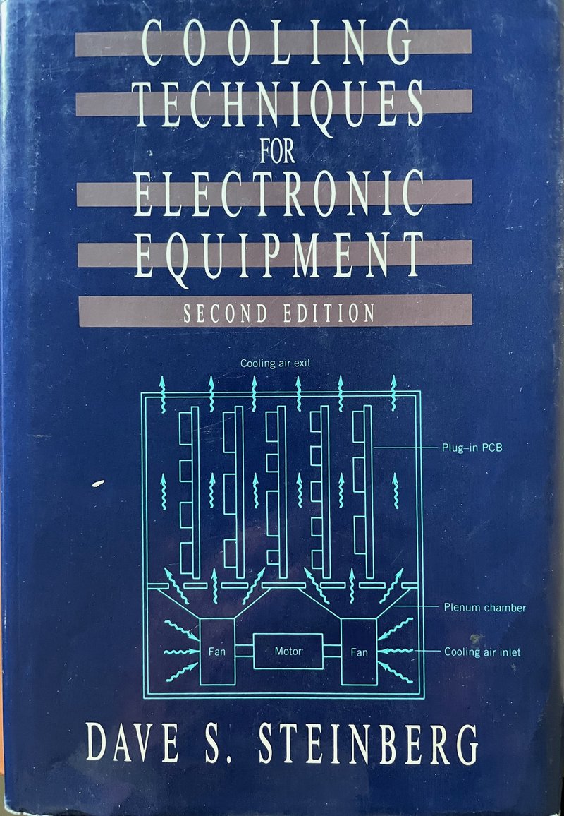
This is a good book for hand cranks
https://www.abebooks.com/9780471524519/Cooling-Techniques-Electronic-Equipment-2nd-0471524514/plp

9780471524519: Cooling Techniques for Electronic Equipment, 2nd Edition - AbeBooks - Steinberg: 0471524514
Details infallible techniques for designing electronic hardware to withstand severe thermal environments. Using both SI and English units throughout, it presents methods for the development of various reliable electronic systems without the need of high-speed computers.
Anyone interested in some trace heating data from a parallel conducting test we did?
![]() I would absolutely be interested.
I would absolutely be interested.
YES!
Discussions
Become a Hackaday.io Member
Create an account to leave a comment. Already have an account? Log In.