 UTFR
UTFRBy: Adam McDonald, Electric Powertrain Design, University of Toronto Formula Racing
Each year, the University of Toronto Formula Racing Team (UTFR) designs and builds a car to compete in international Formula SAE (Formula Student) events. As such, the team must ensure all elements of the vehicle, including the electric powertrain, comply entirely with Formula SAE regulations. This article will discuss the Research & Development project which investigated the possibility of using a new system architecture for the accumulator's temperature monitoring circuitry by outlining the purpose, functionality and design of the revised 'Temperature Motherboard' PCB. All of UTFR’s boards are fabricated in collaboration with JLCPCB (www.jlcpcb.com/RAT), a leading PCB manufacturer providing high quality, reliable, and cost-effective PCBs at a consistently rapid pace.
Purpose and Functionality
As per Formula SAE (FSAE) regulations, the temperature of at least 20% of the cells within the accumulator must be monitored at all times. In addition, all circuits susceptible to high voltage (Tractive System or TS circuits) must be electrically isolated from low voltage circuits grounded to the chassis (Grounded Low Voltage or GLV circuits).
UTFR’s battery management system (BMS) is responsible for receiving and monitoring cell temperatures over a CAN bus; however, the team has implemented Energus cell modules which feature built-in analog temperature sensors that are not directly compatible with the BMS. As such, the voltage readings from the sensors must be converted to temperatures and sent over CAN to the BMS. This is achieved in two stages:
1. A total of 5 In-Segment boards (1 board for each of the five 26-module segments) collect >20% of analog temperature readings, sending the voltage reading corresponding to the highest temperature as the output to the Temperature Motherboard.
2. The Temperature Motherboard receives the 5 total voltage readings from the In-Segment boards, galvanically isolates the signals and sends them to an on-board MCU. The MCU converts the voltage readings to temperatures, and sends the data over a CAN bus to the BMS.
This ensures a sufficient number of cell temperatures are continuously monitored and that the temperature sensors (considered TS circuits) are electrically isolated from the BMS (a GLV circuit) as per FSAE regulations.
Schematic and PCB Design
The schematic and layout of the Temperature Motherboard PCB was designed using Altium Designer. The TS circuity is displayed on the left side of the schematic shown below, with the analog temperature readings received as inputs through JST headers (J1-5). The five analog temperature signals are then each sent through AMC1311 2V unity-gain isolation amplifiers (U2, U4, U6, U8, U10) which isolate the signals between the TS and GLV systems. The AMC1311 chips produce differential pair output signals which are sent as the inputs to TLV6001 general purpose op-amps (U3, U5, U7, U9, U11) to restore each of the 5 analog temperature readings as part of the GLV circuitry.
The 5 analog temperature readings are then sent to an Arduino Micro (U1). A modular CAN node (CAN1) is used to send the collected temperatures to the BMS.
The board also includes 5 B050LS-1WR3 isolated 5V DC/DC converters (PS1-5), which provide isolated power to each of the 5 In-Segment boards.
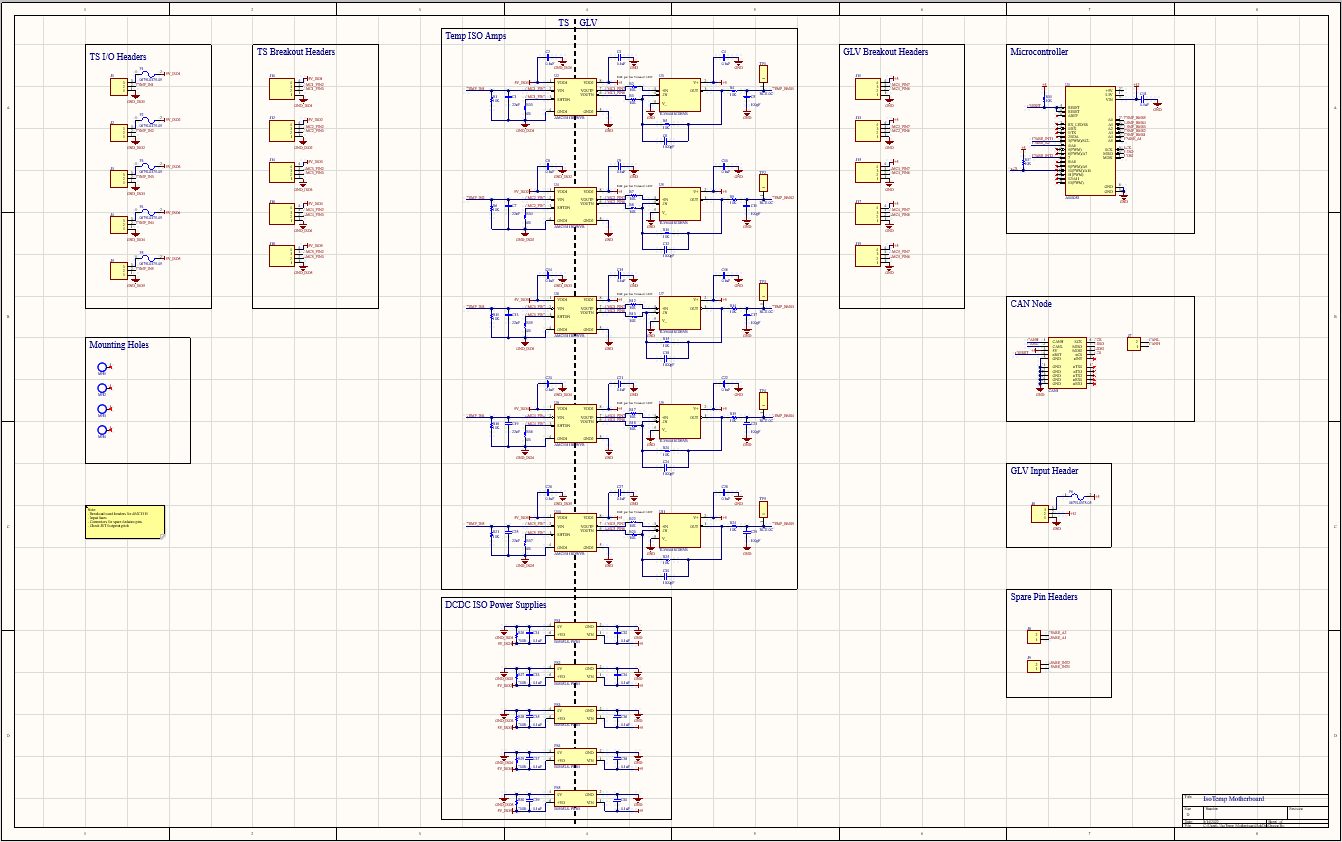
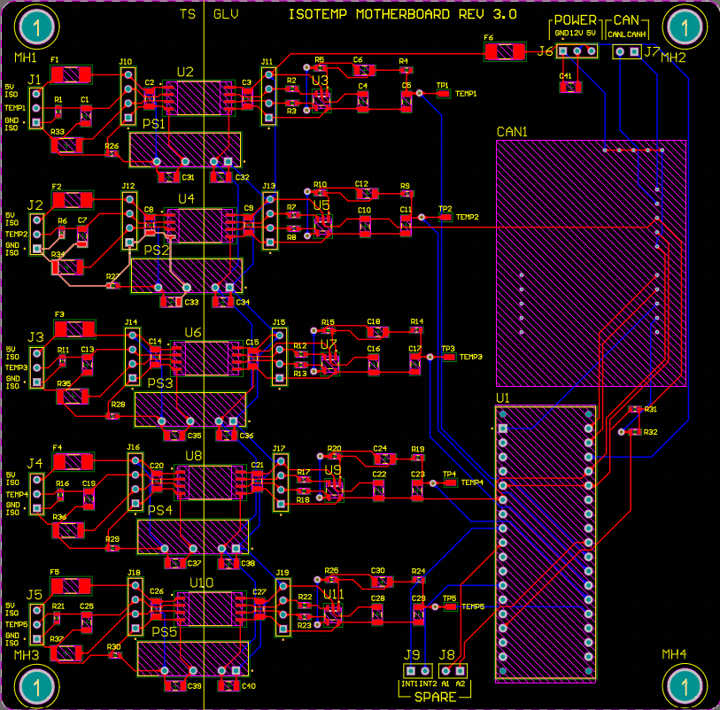
The Temperature Motherboard’s layout separates all GLV and TS circuits, as shown below. The input headers from the In-Segment boards, 5 B050LS-1WR3 chips and 5 AMC1311 chips comprise the left side of the board, labelled TS. The right side of the board consists only of GLV components, such as the CAN module, Arduino Micro and TLV6001 chips, to ensure GLV circuits cannot be exposed to high voltage.
Ordering and Fabrication
The Temperature Motherboard was manufactured with exceptional quality by JLCPCB within days of ordering. If desired, JLCPCB also offers professional SMT assembly with just a 24h turnaround time - more information can be found at www.jlcpcb.com/smt-assembly. The ordering process is remarkably simple:
- Export Gerber files of PCB project
- Click ‘Order Now’ on www.jlcpcb.com
- Upload Gerber files, confirm generated PCB requirements and preferences (including SMT assembly)
- Once all PCBs are saved to cart, proceed to checkout.
Discussions
Become a Hackaday.io Member
Create an account to leave a comment. Already have an account? Log In.