 Avi Gupta
Introduction:
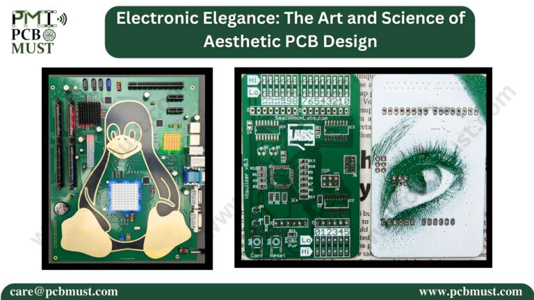
When we think of electronic devices, aesthetics may not be the first thing that comes to mind. However, the visual appeal of a product plays a significant role in user experience and brand perception. In the realm of PCB design, the fusion of art and science creates electronic elegance. In this blog post, we will explore the importance of aesthetic PCB design, the benefits it brings, delve into other key factors to consider, and conclude with the significance of integrating artistry into the world of electronics.
Benefits of Aesthetic PCB Design:
1. Enhanced User Experience: Aesthetically pleasing PCB designs contribute to an enhanced user experience. A visually appealing layout with clear component placement and organized routing improves user interaction and navigation. Users are more likely to feel positively about a device that is aesthetically pleasing, leading to increased satisfaction and brand loyalty.
2. Brand Differentiation: In a crowded market, an aesthetically designed PCB can set a product apart from competitors. Unique and visually stunning designs help create a strong brand identity and differentiate products from similar offerings. This can attract attention, spark curiosity, and ultimately drive sales.
3. Professionalism and Quality Perception: Aesthetic PCB designs convey a sense of professionalism and quality. Well-designed layouts with attention to detail, symmetry, and clean lines reflect the expertise and dedication of the design team. This perception of quality can positively impact a company’s reputation and instill confidence in customers.
4. Ease of Manufacturing and Testing: Aesthetic PCB designs often prioritize efficient manufacturing and testing processes. By organizing components and traces in a visually pleasing and logical manner, manufacturers can easily assemble and test the PCB. This results in improved production efficiency, reduced costs, and quicker time-to-market.
5. Design Iterations and Prototyping: Aesthetic PCB designs facilitate design iterations and prototyping. Clear and visually appealing layouts make it easier to identify and address design flaws or areas for improvement during the prototyping stage. This streamlines the design process, reduces time and cost, and enables faster product development cycles.
Importance of Aesthetic PCB Design:
1. Component Placement and Organization: Aesthetic PCB design involves thoughtful component placement and organization. Considerations such as proximity of related components, clear labeling, and logical grouping contribute to a visually pleasing and functional layout. This helps improve signal integrity, reduce electromagnetic interference, and simplify maintenance and repairs.
2. Trace Routing and Optimization: Aesthetic PCB design incorporates optimized trace routing techniques. Proper routing ensures efficient signal flow, minimizes crosstalk, and reduces electromagnetic emissions. Additionally, careful attention to trace widths, lengths, and spacing can improve signal integrity and impedance matching, leading to better overall performance.
3. Color and Contrast Selection: Aesthetic PCB design includes careful consideration of color and contrast. Choosing contrasting colors for different functional blocks, using color-coded labels, and utilizing silkscreen printing effectively enhance the visual clarity of the PCB. This aids in component identification, troubleshooting, and overall aesthetic appeal.
4. Enclosure Integration: Aesthetic PCB design takes into account the integration of the PCB within the product enclosure. Aligning connectors, switches, and indicators with the overall product design ensures a seamless and harmonious integration. This creates a cohesive and visually pleasing end product.
5. PCB Size and Form Factor: Aesthetic PCB design considers the size and form factor of the PCB. Minimizing the PCB footprint, reducing unnecessary spaces, and optimizing the component density result in sleek and compact designs. This enables the creation of smaller and more portable electronic devices.
Other Factors to Consider:
1. Design Constraints and Specifications: Aesthetic PCB design must adhere to the specific design constraints and specifications dictated by the project. This includes factors such as power requirements, signal integrity considerations, thermal management, and regulatory compliance. Balancing aesthetic appeal with functional requirements is crucial to ensure the PCB meets the necessary standards.
2. Design Tools and Software: Utilizing advanced design tools and software aids in achieving aesthetic PCB designs. Design software with intuitive user interfaces, 3D visualization capabilities, and design rule checks allows designers to create and verify aesthetically pleasing layouts. These tools also facilitate collaboration between design and manufacturing teams.
3. Collaboration with Industrial Designers: Collaborating with industrial designers can elevate the aesthetics of the PCB design. Industrial designers bring expertise in product aesthetics, ergonomics, and user-centered design principles. By working closely with industrial designers, electronics engineers can create PCBs that seamlessly integrate with the overall product design.
4. Environmental Considerations: Aesthetic PCB design should take into account environmental considerations. This includes using environmentally friendly materials, designing for efficient energy consumption, and ensuring recyclability at the end of the product’s lifecycle. Incorporating sustainable design practices aligns PCB aesthetics with the growing focus on environmental responsibility.
5. Design Documentation and Communication: Comprehensive design documentation is crucial in aesthetic PCB design. Documenting design choices, including color schemes, component placement rationale, and routing strategies, aids in maintaining design consistency and effective communication with manufacturing partners. Clear and detailed documentation ensures the intended aesthetic vision is accurately implemented during production.
Conclusion:
Aesthetic PCB design merges the art of visual appeal with the science of functional electronics. By prioritizing component placement, trace routing optimization, color selection, enclosure integration, and PCB size considerations, designers can create visually stunning and high-performance electronic products.
The benefits of aesthetic PCB design extend beyond the visual appeal. It enhances user experience, differentiates brands, conveys professionalism and quality, simplifies manufacturing and testing, and streamlines design iterations and prototyping.
Considering factors such as design constraints, collaboration with industrial designers, environmental considerations, design documentation, and effective communication are essential in achieving successful aesthetic PCB designs.
By embracing the art and science of aesthetic PCB design, electronics engineers can create products that not only function flawlessly but also captivate users with their elegance. Aesthetics and functionality can harmoniously coexist, resulting in electronic devices that inspire, delight, and leave a lasting impression. Let us embrace the world of electronic elegance and create electronic designs that captivate the senses.
About the Author:
Avi Gupta, Founder of PCB Must Innovations, is a dynamic force in the world of electronics design. With a wealth of industry experience, Avi thrives on solving intricate problems and delivering dependable solutions. A tech enthusiast, Avi stays ahead of trends while cherishing precious moments with family.
Avi could be reached at care@pcbmust.com
Discussions
Become a Hackaday.io Member
Create an account to leave a comment. Already have an account? Log In.