 Eric Hertz
UPDATE -- New SOIC-breakout... see below.
Working on a solderable-prototype... due to solderless-breadboard-wiring-wonkiness.
Decided not to design a full-on PCB, yet, as it's still in the prototyping-stage...
Decided on 70mm x 70mm boards, they're much cheaper than the width necessary for a DIMM, so I'll "cludge" two together... It's actually pretty easy and stable with thin PCB-material to just overlap them for one or two rows.
So, the board design is somewhat generic.
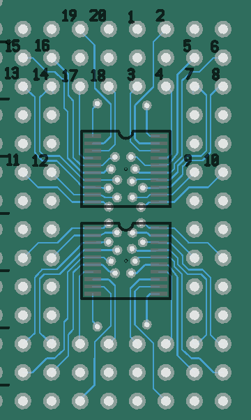
First things first, the DIMM socket will solder into two 70mm tall boards with this running from end-to-end:

Might take a little hand-drilling for the support-mounts, etc. But I'm more than OK with that.
The thing about the DIMM sockets is that they have this weird footprint with diagonals... more on that in a bit.
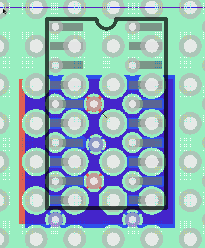
Next we have some breakout for surface-mount chips, since 7400's in the speeds we're looking for mostly only come in SSOP, or if you're lucky (as a prototyper) SOIC.
(Yes, this is a breakout, for prototyping. No these traces are not matched-length, and who knows what kind of signal-issues may arise due to their closeness to each other).
Now, you might look at that layout and go "whhhaaaa??!"
But check this out... If I'mma make a prototyping-board and have ten of 'em made, I'mma think of other projects as well... So the above was designed *after* (on the other side of) this:
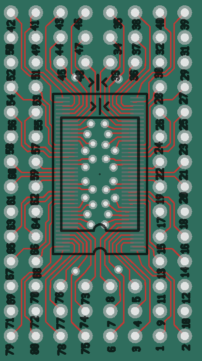
I don't actually have any SSOP80 chips, that I'm aware of, but I do have some TSSOP56's I'd been planning on using... So this'll break that out nicely, and leave room for later prototypes.
(If you have better ideas how to label the "pin numbers" to accomodate an arrangement like this, I'm all ears. I've thought about A1-A9, B1-9, etc... just to make it clear that these numbers *don't* correspond to the pin-numbers on the likely-smaller chips that'll be installed. I know better, but've been caught slipping-up on TQFP100 adapters fitted with smaller devices).
Again you might say "whhhaaa?!" at the breakout-layout/numbering... Herein, the layout is specifically-designed to occupy as little space as possible while *also* being easily "straddled" with a 32-pin DIP, or even 40-pin, yahknow, with a few extra holes at the ends.
So, that may seem a bit ridiculous, but consider sdramThingZero's parts-tally so far... We've got a 40-pin DIP (AVR), a SSOP-20 (74xx574 latch), and two SOIC-14's (74x00 NANDs). (Though, since this's been designed, I might opt for SSOP-14's in future orders). And, again, consider that this single board-design will be used *twice* to handle the DIMM socket... On one board, I can throw the AVR over the above layout and not waste a whole bunch of holes under the DIP.. On the other board, I can already handle two of my three 7400-series chips... again in that same workspace.
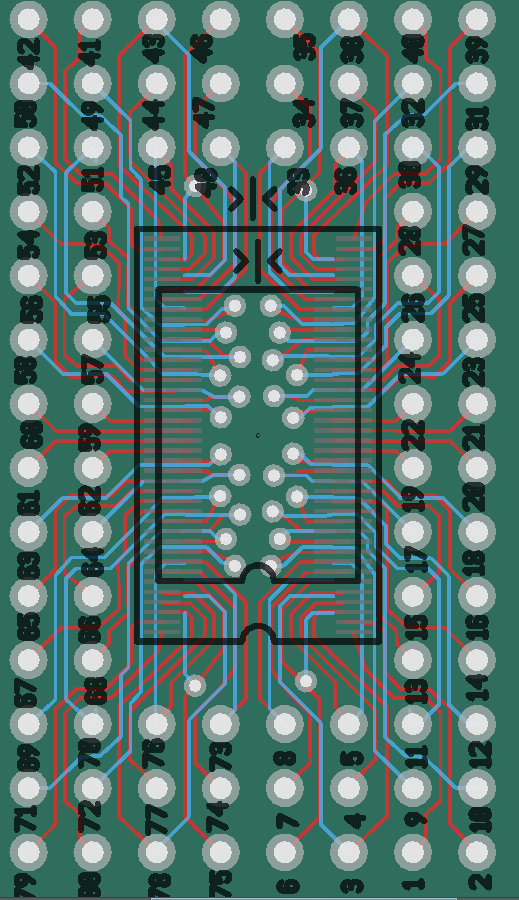
And, I'm currently working on a more generic SOIC-breakout... Which isn't too-difficult considering they're half the space of regular breadboard spacing... meaning that when they're not populated, that space can be used as regular 'ol breadboard:
So, the SOIC can be placed, it's a bit easier to solder to a via than directly to a pin... and it makes for backside-wiring, which I usually prefer. Note, again, if I don't need to place a SOIC, then that entire space can be used just like regular ol' 0.1in breadboarding-space. Should also work quite well with e.g. SOT-3, no?
Then, there's the "center vias" I thought Ted was talking about in the comments, below... But he was talking about different ones. These center-vias alternatingly attach to "planes" on the top and bottom layers, making it easy to essentially have power and ground-planes on a 2-layer board, and easy to "solder-blob" most pins directly to 'em, or insert surface-mount decoupling-caps, pull-resistors, etc. on the back-side.
Debating the use of octagonal vs circular pins/vias... also experimenting with the planes' violating the DRC trace-width rules...
---------
So, this, like all my soldered-breadboard prototypes, will be wired point-to-point with "wire-wrapping" wire... (Though I may try out enameled-wire in the future). It's pretty easy to do when you've got plated-through-holes to solder-to...
Here's an old project, #audioThing pretty small.(I know I've some better examples, but camera's not reachable, and these are the best I've found online...)
Note that I used two overlapping pieces to achieve that shape... just as I intend to do with this project. In that project, the DIP socket actually serves as a bit of structural-support for the overlap. In this project, the DIMM socket will do the same, but I'll probably also solder in some scrap-wire (or resistor-lead cuttings?) through all the remaining overlapping holes... "stitching" the two boards together. (On that note, maybe I won't overlap them, but instead will stitch them together side-by-side? Hmmm, not sure I'll be getting the holes perfectly-spaced with the edge for that... Though I finally have a nibbler-tool again!).
Another project-idea makes use of some funky-connectors with spacing very similar to the PCB-footprint of SDRAM, so another "two-birds-with-one-stone" scenario...
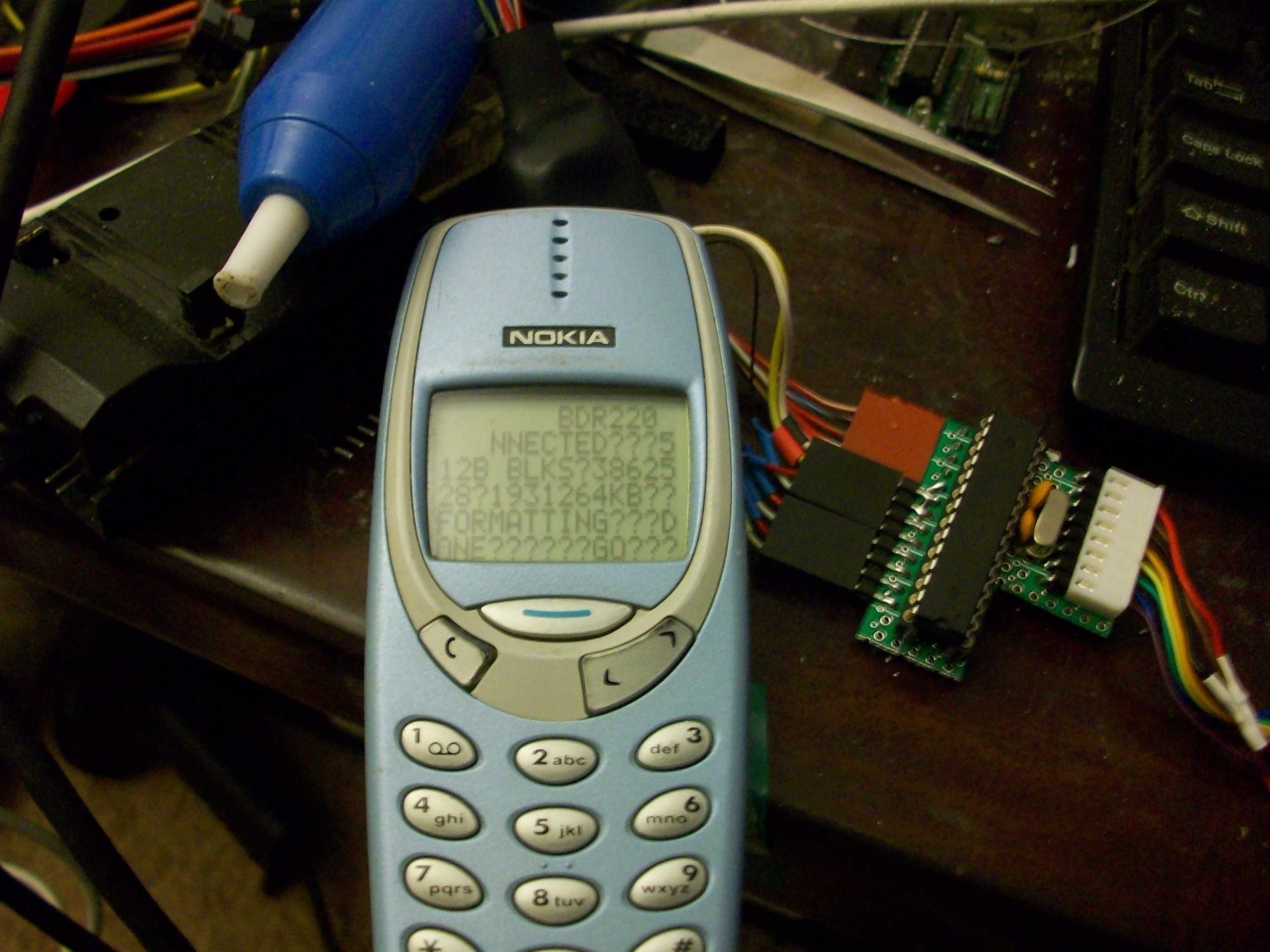
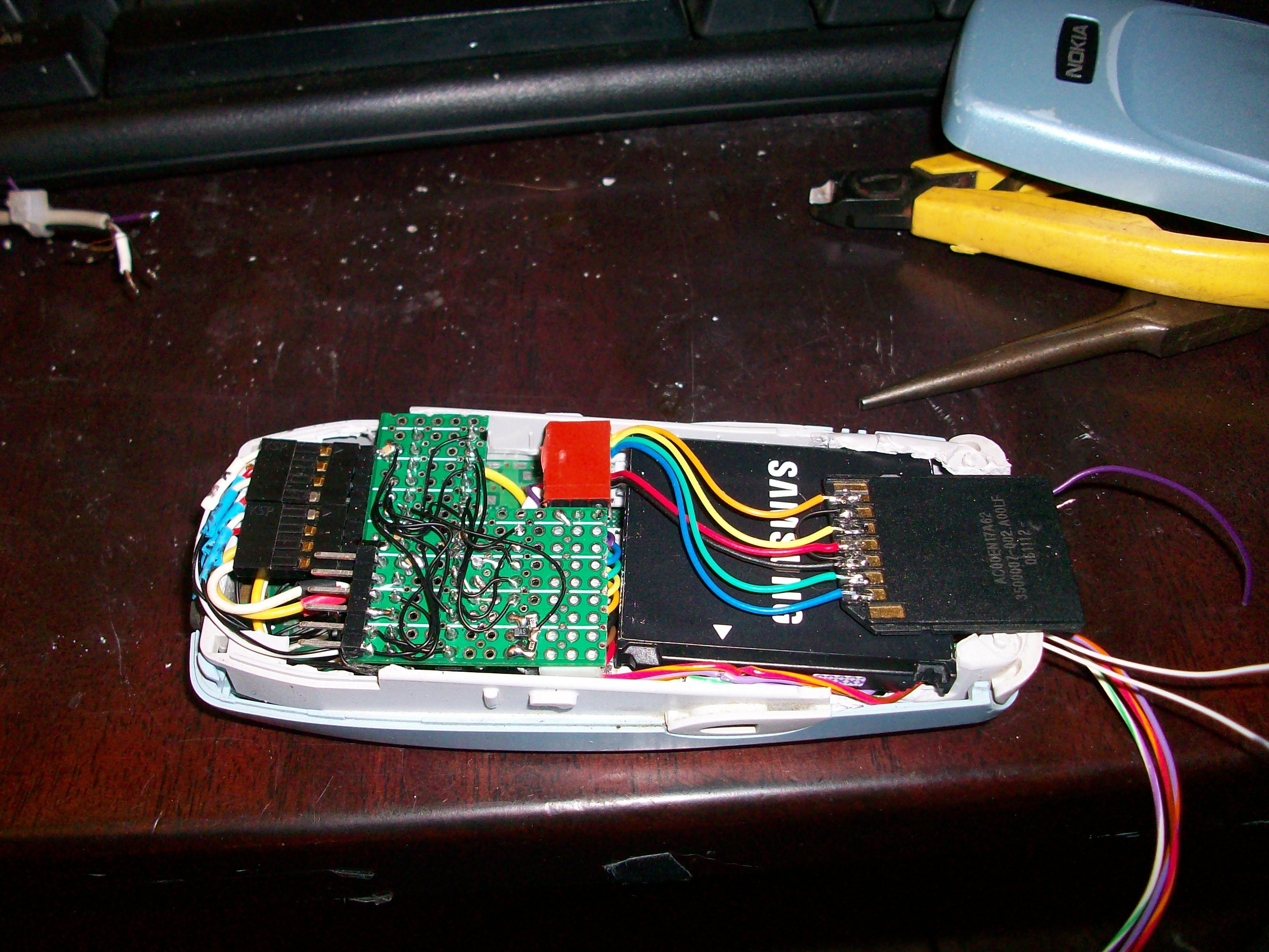
This guy's an early-early prototype of that... Well, it was *supposed* to be an "early-early prototype" but it's been running for two years now, used daily... so don't balk at its ugliness ;)
 Note the black connector on the left... Its mate *did* have very-similar (diagonal) footprint-spacing as my DIMM-socket, until I forced it to fit in regular ol' 0.1in (square) breadboard. It was not easy, but it does work. That'd be much harder with a DIMM-socket since, among other things, it's got more than 5 times as many pins... And that's not the real kicker... The real kicker is the fact its pins aren't in 0.1in "columns" but 1.6mm, instead. So, 0.1in "rows", but four 0.63in columns. *really* hard to stretch-to-fit on 0.1in spacing... thus the main reason this new proto-board is being designed in the first place.
But, I think the connector finagled in the image above would be *much easier* to finagle into the DIMM-socket's diagonal spacing than it was on 0.1in (square)... So, again, kinda two-birds-with-one-stone.
And...
I dunno about you, but solderable-breadboard is one of those things I use even in tiny pieces... I've cuttings saved-up that are only two 0.1in-spaced pins... These are handy for e.g. adding strength to snap-apart headers, when they're not soldered-directly to a PCB... Or yahknow some of those headers that the pins slip in-and-out of... or maybe you're putting an LED on a panel-mount and need an inline-resistor that happens to be surface-mount... Breadboard-scraps of all sizes are just handy to have around.
So it strikes me as somewhat surprising I've never heard of "breadboard-grab-bags" from the ol' PCB-manufacturers... surely not everyone makes perfectly-square PCBs that interlock perfectly with all the other boards being fabbed at the same time...
This shot is from https://hackaday.com/2016/10/15/look-what-showed-up-for-bring-a-hack-at-osh-park/

Might be hard to squeeze too many DIP-40 sized breadboards out of these scraps, nevermind needing to add an extra CNC-mill path... But I imagine they've all sorts of shapes/sizes of scrap from *between* boards that could be filled with 0.1in spaced holes. Maybe even oddities like 2mm-spaced... or even some random oddly-shaped SOIC/SSOP-breakouts... A script just randomly throws some useful stuff in whatever space is left-over between boards... don't bother milling them to a specific shape. What're yah gonna do with that crescent-moon-shaped breadboard? Mini Grab-Bag with every order, or "The Big Grab Bag" for $1.00...
(You'll note my boards aren't in purple... I haven't yet ordered boards from @oshpark... How would y'all feel about an order for 10 70mm x 70mm boards with nearly 1500 plated-through-holes on each...? More importantly, how would yer drilling-robot feel about it?)
Discussions
Become a Hackaday.io Member
Create an account to leave a comment. Already have an account? Log In.
@esot.eric if you send the send file to support@oshpark.com then we can take a look and let you know. our general guidelines: http://docs.oshpark.com/submitting-orders/
Are you sure? yes | no
Awesome, thanks for the info! I don't see any mention regarding number of drills... but this has got a lot of 'em! Probably wise to check with support, before ordering.
Are you sure? yes | no
Hi - I've just confirmed that there is no maximum number of drill hits. They just can't be overlapping.
Thanks,
Drew Fustini
<drew@oshpark.com>
Are you sure? yes | no
Thank you for looking into this, Drew! That's great info.
Are you sure? yes | no
I approached OSH Park about packing #Ugly SMD Adapters into interstices between paid boards, and they said they typically have *no* space left on a panel; their placement process - whatever it is - is that good. I'm not sure if it's automated (seems like a knapsack problem to me), or manual, or a combination of both.
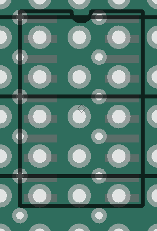
The vias in the center are there to connect the top and bottom IC footprints to the through-hole pads?
Are you sure? yes | no
Hah, yeah, those are some small adapters, good point, in there, about normal adapters' through-hole-plating shorting out with Manhattan-style ground-planes. That'd've been pretty slick if they went for it! Heck, looks like several could be fit in those "frame" scraps... Even as-is, that stuff'd make for good Manhattan-style material, eh?
Otherwise, I imagine they do their darn-tootinest to fill up the boards as best they can...
The vias in the center are no longer to be discussed per fears of CNC-drilling-robot uprising.
"What, you're too lazy to add another wire? So, instead, you make us drill 700 extra holes?! I'll show you what laziness will getcha!"
...or do you mean the ones on the SOIC-breakout...? No those ones are merely to feed the signals to the bottom-side, it's easier to tack a wire onto a big ol' solder-blob than to do-so on the SOIC's pins, directly.
Are you sure? yes | no
oy, mind's fading... But just reread your question, and now I see you mean the vias in the center of the *IC footprints*...
Those are there because with 6mil trace/space I couldn't fit the TSSOP-80 nearly as compactly as it is with all the traces on the same side... mainly. Secondarily, they just happen to work out somewhat-nicely for the TSSOP-20's on the other side. Was a nice surprise, more than anything. Actually, I'd planned to place the order long before I even came up with the idea of throwing the 20-pinners on the back. It only took a tiny bit of revision to add 'em. Nice surprise.
Are you sure? yes | no
On that note... there's a new image showing the top-side traces only, you can probably see how difficult it would've been to route without the vias
Are you sure? yes | no