 Eric Hertz
(UPDATE: Multiple DIMMs now functional... inverted clock-signal. See bottom)
The last log had a bit of a "scare" regarding the clock-signal, shielding, etc.
It's really not that big a deal. I replaced that long-shitty wire with a shorter and (by feel) higher-quality one... and the problem is resolved.
So, the end-result, which I'll throw in the "instructions" if I remember, is:
The first likely point-of-failure would be connectors/connections.
The second likely point-of-failure is a shitty clock-line, which could probably be fixed with little more than using a high-enough-quality shielded-wire. Maybe headphone-wire isn't enough, but if you've scrapped an old laptop with WiFi, you've got a nice thin and certainly high-enough-quality shielded-wire right there.
OK, now I've tried out several DIMMs, and have had luck with two different modules. One's 4 chips on one side, the other's 16 chips, two-sided. (The second side is not-yet-supported). The other DIMMs (all remaining are older-model 16 chippers) seem to *almost* work, but printout (via serial port) is garbled, leading me to believe these older modules might be drawing too much current from my clock-source.
I've got a 32MB (4-chip) (VIS?) and a 256MB (16 chip) (Micron) (Only one side supported: read as 128MB) functioning.
NOTE: For a double-sided DIMM, it's (currently) necessary to tie /S1 and /S3 high. If left-floating, the back-side chips may try to drive the DQs at the same time as the front-side chips! TODO: Shit, wasn't there another I pulled high, with a resistor? What was that...?
Determining the size of the chips (without using the SPD) turns out not to be too difficult... I haven't verified this is within-specs (it requires that the dimensions are 2^n, and that addressing something higher causes wrapping). But the basic idea is simply:
- Write to the column-address with the highest-possible address-bit set... (e.g. A0-A12 are implemented, so write to column-address 4096, in row 0, bank 0)
- See whether column-zero was modified
- Repeat 1 and 2 with the next lowest address-bit set (address 2048, 1024...)
- UNTIL: column-zero was unmodified.
- When column-zero was unmodified, you know your size.
- e.g. it was modified when writing to 1024, but not when writing to 512, so each page is 1024 bytes (ending at column 1023)
The same can be done for rows... (always writing at column 0).
Interestingly: I can't explain this...
Using the same read/write code, one DIMM reads-back at (or writes to?) a different address than the other. So, e.g. I write a value to column 3, and for one DIMM I can read it back from column 3, but the other I have to read column 4!
Strange, as they both have CAS-Latencies (available at, and) set to 3... and otherwise the chips must follow the same timing-specs, right? (Others, such as DQM-Latency are not configurable, nor reported).
In general... it doesn't really *matter* whether we request column-0 and wind-up getting column-1 or column-1023, as long as the reads and writes are aligned to the same offset. And, I've managed to figure out how to auto-detect the offset.
BUT: with free-running, it's a bit different... Essentially, the "Read" command from the free-runner (telling itself to read-burst the next page) is handled *differently* than the "Read" command from the "host"... Because... the Free-Runner's Read-command is fed-directly-back to its command-inputs, there's no need to DQM, change bus-directions, etc. which are all necessary when the host requests a data-read. So, then, if the Free-Runner requests a read starting at column 0, it will, most-likely, start at column-0. Now, let's just pretend the host's read/write "offset" is +1... So writing to "column-0" actually results in writing to column 1... Then writing to 1023 actually results in writing to column 0. Now... Say (and this is a bit simplified) column 1023 is loaded with the "read-burst next page" command.... But, that's actually, mistakenly, written to column 0, from the host. Now, during Free-Running, the "read-burst next page" command occurs *immediately* after read-bursting the previous. We only get Column-0 in each page, rather than Column-0 through Column-1023.
So... somehow... I *have* to find out which column is *actually* column0, regardless of whether the host-reads/writes are aligned and accidentally *calling* another column "column-0".
Again, it doesn't make sense to me that they're *not* actually aligned with zero offset, both read and write. I followed the timing-diagrams/explanations darn-near exactly. Except (of course) that this particular procedure isn't explicitly *described*, it still falls within the specifications. So... huh.
When the SDRAM clock and the "Host" clock are synchronized, it's not exceedingly-difficult to determine the actual offset; start free-running, and read-back the values it outputs while it's running. But that's not possible when they run at different speeds... So... huh.
The one thing I can think of off-hand, is that there's something to do with the delays between, e.g., the AVR's output-changes being received at the SDRAM (via long wires) and the clock-edge. Why would this affect one DIMM and not the other...? If the set-up time is *right* on the threshold, it's plausible.
Here's my timing-Diagrams:
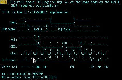
WRITE:
READ:
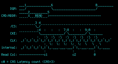
Note that for everything other than the /CS strobe (steps 3 and 4) and the CKE strobes (7,8 and 9,A) the timing shouldn't be important (e.g. between step 1 and 2 there could be several clock cycles)
TODO: Verify against the ATMega8515 timings:
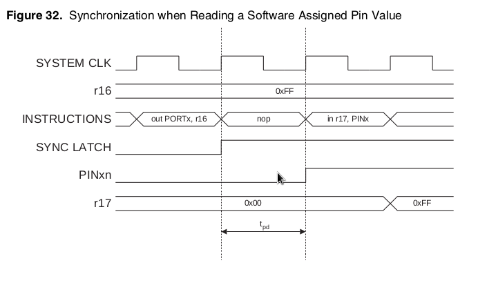
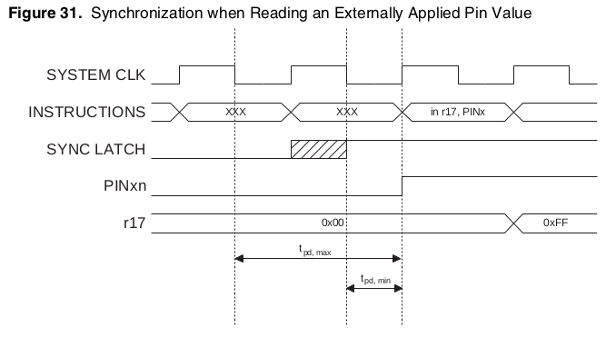
(No diagram for the PORT output... I guess that's Figure 32's SYNC LATCH, which appears to change on the rising edge of the clock... And with different-length DQ wires vs. the clock, might interfere with set-up time... Maybe I should run the AVR on an inverted-clock signal... Again, I'm just using an AVR, at this point, because I know its timing is *precise*; each assembly-instruction occurs sequentially, when interrupts are disabled there's no risk of unexpected delays from e.g. caching or branch-prediction used in more powerful uC's. Also, it has a *bunch* of pins. Later, this will be implemented with explicit register-ICs, and one-shot circuits, to interface with the "host"'s completely asynchronous bus. )
I *think* I ran into some of these problems (unexpected offset) with #sdramThing4.5 "Logic Analyzer", but for that version, and all prior, I was unable to swap out the DIMMs, so just hardcoded whatever value worked... Now, I guess, it's about trying to figure out what's going on, so it'll work with more DIMMs)
Update: Sho' 'Nough! Inverted the clock signal to the SDRAM (physically easier than inverting to the AVR due to breadboard layout).
Now I've verified functionality with 5 of 7 of my DIMMs, of various manufacturers from 32MB to 256MB.
(I'm running this entire circuit, including the DIMMs--some dual-sided=16 chips--off my FT2232H breakout-board's 3.3V regulator... so it's entirely plausible the other two DIMMs are just drawing too much current. Haven't looked into it yet).
(Would you believe I got away with running a TI SN74LS04N off 3.3V? 16MHz, clean enough for clocking SDRAM... And get this, the date-code is 7945A... 1979, yo!)
And, now they all have the same read-vs-write column-offset (before, of the two functional chips, one had an offset of 0 and the other had 1. Now they all have an offset of 1, which is probably explained by the clock-shift, or maybe the AVR's PIN-latching scheme, and suggests maybe my timing-diagrams were correctly-designed.
I'll be looking into that later, the cat's telling me it's time for bed.
(Interesting side-note... on prior versions of sdramThing, definitely up to sT4.0, maybe even 4.5, I didn't invert the AVR's clock. According to what I can find, the AVR changes its outputs on the rising-edge of the clock, the same edge that the SDRAM samples... I musta been running *right* at the threshold of the set-up and hold times! Amazing those previous versions worked as well as they did. I can't recall if I tried an inverted-clock when doing all the high-speed clocking experiments with #sdramThing4.5 "Logic Analyzer", but I got that running up to 30MHz before it started having issues... A gajillion factors probably contributed to that limitation, but if I didn't eventually invert that clock (and carry that inversion through to the one-shots, etc.), it makes me wonder if I could've gotten even more out of it.)
Discussions
Become a Hackaday.io Member
Create an account to leave a comment. Already have an account? Log In.
This is so neat... I'm really enjoying following along on this.
Are you sure? yes | no
Thanks, yo!
Are you sure? yes | no