 Eric Hertz
The address thing of the past few logs is... cool-that-it's-possible. If you don't recall from a while-back, the idea was to use a *default* address-location to use as a jumping-point to all other address-locations.
A bit simplified, I'd write to address 0 *the address* that I want to jump-to/write-at/read-from, then I could use the SDRAM's address-0 as, essentially, the "latches" necessary to latch the address from the bus.
It would take a bit of fiddling, and a lot of software, but it's doable, I'm pretty sure... like 98%.
And, it'd be cool!
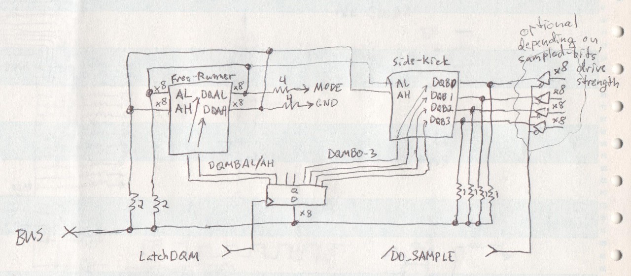
Doing-so, I've determined, at the least, would require resistor-networks to connect the address-pins to the bus (resistors marked "2"), and buffers connected to a "default" address, with output-enables. These buffers would have to be inserted between the resistors marked "4" and DQAL/DQAH, much like the similar-arrangement seen at the "Side-Kick."
So, then, one control-signal connected to those buffers' output-enables would load the "default address" (which actually, wouldn't be 0, but that doesn't matter to this functionality) and that same signal would disable that default-address when the data-lines attached to the address-pins are driving the *actual* address I want to access.
I'm still kinda partial to it, but it would be a bit slower, and still requires two 8-bit (buffer) ICs which could easily just be replaced with regular ol' latches (and a couple additional control-signals).
But, again, it'd be a bit slower, slowing *nearly every* command between the host and the "Free-Runner" (every command that requires an address, except "Load Mode Register" which is a one-time deal on init) by quite a large factor.
E.G. to read from row 200, column 1000, would first require writing "200" to "address 0", then reading-back the "200" from address-0, then issuing the "Activate Row" command. But, we haven't yet issued the *read* command, from column 1000, so we repeat the process loading "1000" into "address 0", then reading-back the "1000" from address-0, then issuing the "Read" command. That's a *LOT* to do that could easily be accomplished with a couple 8-bit latches.
But, unquestionably, I'm partial to the idea.
--------
That said, I've kinda put it on the back-burner, thinking instead about the *easiest* way to whittle 20+ control-signals and 32+ data-bits down to an 8-bit bus. And, I think I'm at about 80% complete on how to do-so, using Latches, and (likely) those resistor-networks at the "Side-Kick" for its 32-bits.
Here, again, is the *current* circuit, as-implemented and currently running (The side-kick has not yet been reimplemented... that's easy-enough).
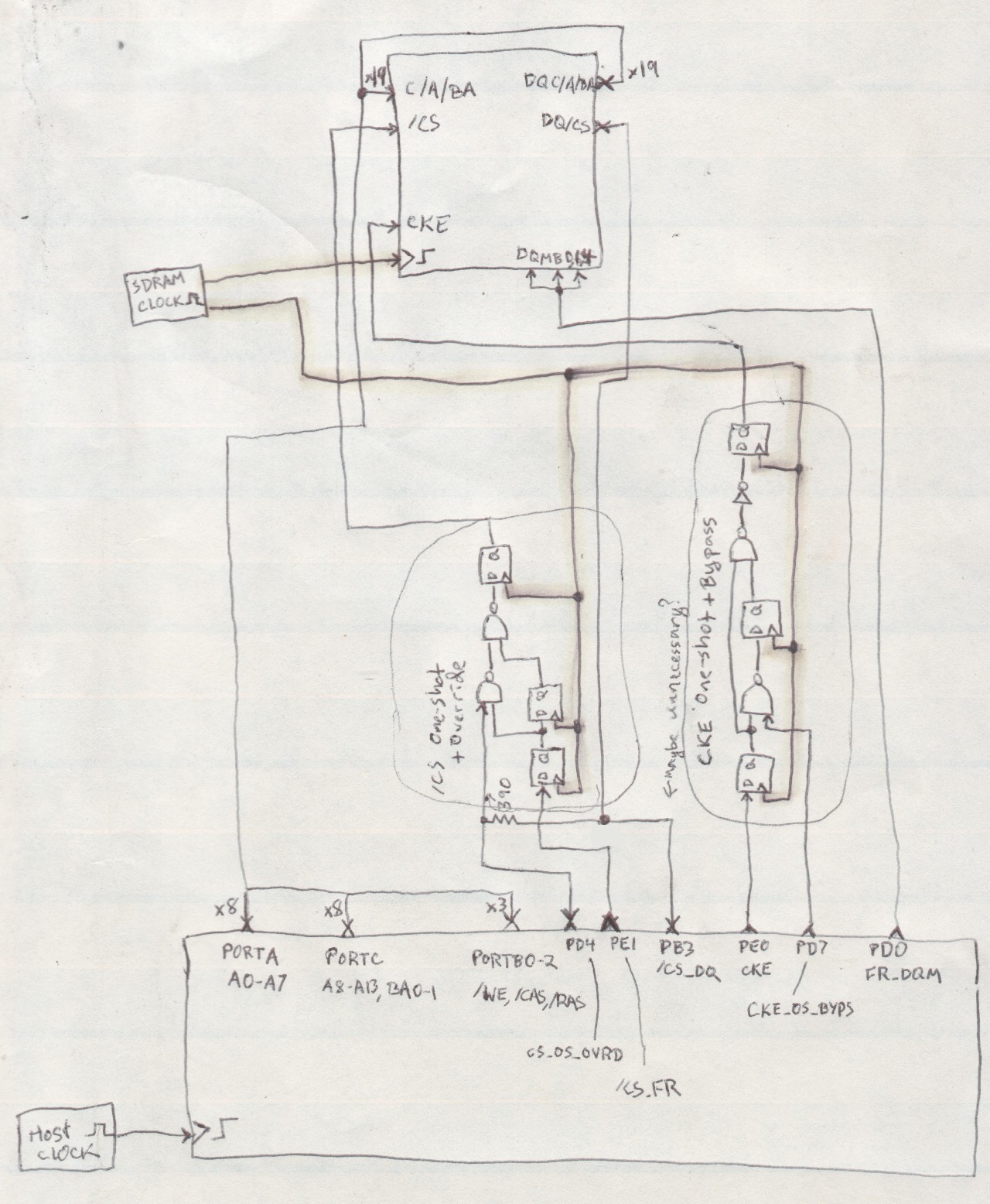
The controller at the bottom is an AVR (ATmega8515)... but it's basically just treating all the I/O's as GPIOs, not using any special features/peripherals... So it *could* be implemented on *any* controller with enough GPIOs (and program-space).
Again, the purpose of the One-Shot circuits is to allow your "host" to communicate with the SDRAM at whatever speed it's capable (as long as the SDRAM clock is faster than your host's GPIO-toggling).
So, basically, as it stands, as long as your host has enough GPIOs, and can be programmed in "C", there's not much to be done to port what I've already accomplished to another host.
So, it's a bit silly to fixate on this "Bus" system, at this point, as the circuit's already-functional As-Is.
But I'll come back to that...
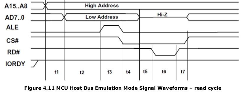
Here's the basic idea of the "bus" system... I'm planning on making it compatible with the 8051-style bus... that guy's pretty common-place and easy-enough to implement via GPIOs, if not already directly-supported by your "host".
Here's an example from FTDI's FT2232H datasheet:
Several AVRs also implement this protocol (e.g. my ATmega8515), PIC32 supports it on its "Parallel Master Port", and of course it's also available on the 8051-series. And, again, kinda cool, the FT2232H supports it, which means you could connect sdramThingZero to your computer, or Pi, or whatever via USB2.0 without even touching a microcontroller.
I wouldn't be making use of A15-A8, nor /CS, nor IORDY. The latter-two are not available on all "hosts", and A15-A8 aren't necessary for my implementation.
Here's a *quick* look at how it'd be implemented...
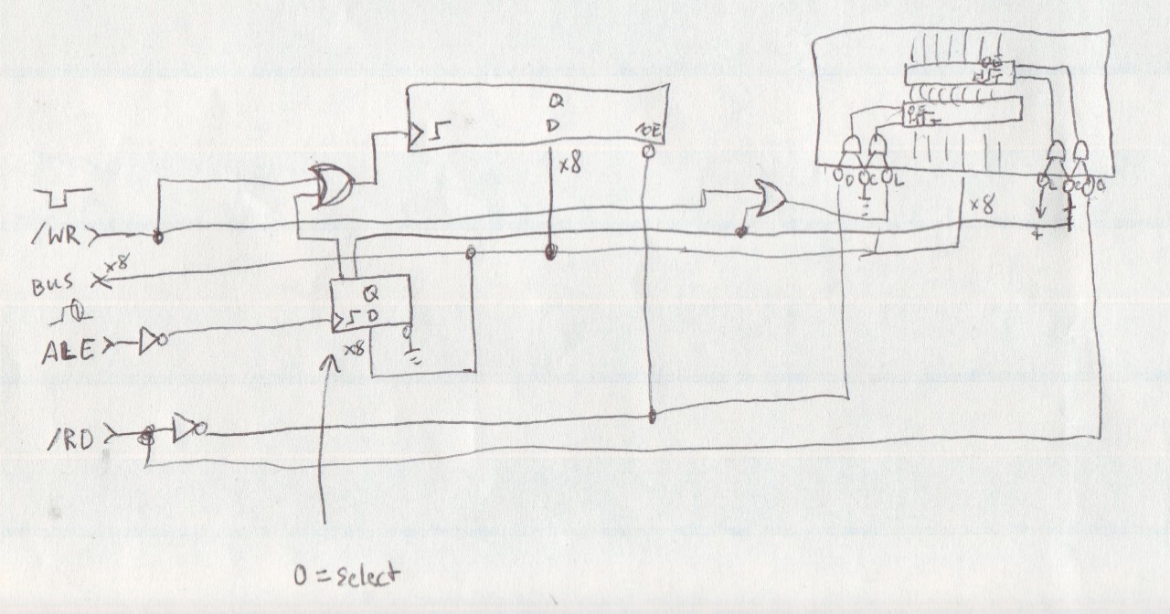
There are two parts shown, the DQ-latch on the top-left is e.g. a 74AHC574. The one on the right is e.g. a 74AHC543 *bidirectional* latch.
If you look again at the as-implemented circuit, you'll note there are some signals which are one-directional (output to the SDRAM, only) and some that are bidirectional... Before the '543 was brought to my awareness, the original idea was to just use resistor-networks and '574s. It'd work, but maybe a bit less-intuitive.
The DQ latch at the bottom, connected to ALE, selects *which* latch you wish to read/write.
So you're not *addressing* the SDRAM, you're addressing the Latch. In a way, I guess, this whole system is a bit like a "port-expander" ala the 8255. (Though they seem to still make derivatives of that chip, I have yet to find one that can handle 100+MHz... and, besides, the glue-logic vs. "epoxy-blob" technique is a bit easier to wrap my head around).
-------
Anyways, I think it'll do just-fine. And, if you happen to be working with GPIOs rather than an actual 8051-style bus-peripheral, then there are things one can do to speed up the read/write process (making use of Bursts, etc).
---------
Running out of steam on this writing...
Earlier, the idea occurred to me... This system is basically-functional, as-is. Before the bus-expander, before the address-scheme...
Maybe it makes sense to just document it *as-is*, make instructions leading up to this point, and upload the software. And, maybe even design a PCB *at this point*, considering the bus-expander as a sort of add-on.
There's a *little* bit to be done regarding the side-kick, but not much.
I have a few PIC32s with high-pin-counts and lots of program-space that could do the job... And there's no reason it couldn't be accomplished with a high-pin-count/large-program-space AVR, as the code is already designed for AVRs and 98% architecture-agnostic. And, for now, just send the sampled-data to a computer via a serial-port. Slow, yes. And Not Yet Pi-compatible. But *completely functional* and repeatable (and probably more easily-understandable) should anyone so-desire.
(TODO: Trigger-input... ONE SDRAM-address-pin fed-through a MUX? Instead, a second /CS_DQ? (and easily-implemented circular-pre-buffer!))
Discussions
Become a Hackaday.io Member
Create an account to leave a comment. Already have an account? Log In.
As usual, I'll stick in my 2 cents... As I've said before, I think it's less important that it be stand alone hardware, and more important that it works well. Using an high pin count uC to "get 'er done" is a good choice, in my humble opinion. I'd be more worried about the things that are needed to make it /useful/ and less worried about the things that could make it "cooler" or simpler or whatever.
Specifically:
- that trigger is /critical/. And it would really be "cool" to have /complex/ triggers. This is why I keep going back to something with an FPGA or like that. Wait! Before you react to my suggesting that /yet again/ (LOL) please hold on and understand: There are processors out there which have high pin count IO ports, with a standard uC core... AND have an FPGA section. Please... please, please... take a look at the PSoC and TI Tiva uC's. They are low cost, well supported, pretty easy to get started with (compared to other processors in their space... they are more complex than PIC's or AVR's) and would be /ideal/ for this application... while at the same time allowing for future expansion to make use of the programmable logic.
You can get a dev kit for next to nothing, e.g. the CY8CKIT-049-42xx with 4.5 8 bit io ports at digikey for $4.00 (FOUR dollars!) and have an ARM core, gobs of IO, serial, SPI, I2C, etc... and... 4 blocks each containing 2 PLDs which are easy to configure with their graphical development package
http://www.cypress.com/products/32-bit-arm-cortex-m0-psoc-4200-programmable-digital-blocks
http://www.cypress.com/documentation/development-kitsboards/psoc-4-cy8ckit-049-4xxx-prototyping-kits
The TI Tiva is interesting to me, because as far as I can tell, it's the only processor out there that comes with a USB ready bootloader built into the chips ROM. So you can populate boards in China, send them directly to the customer, and then send them files to program the units, eliminating the need to have firmware done before project completion, or to re-ship after loading firmware. It's a competitive advantage. But the CCS IDE is harder to work with, and TI doesn't do as good a job with supporting little guys like us. It's still doable...
Anyway... sorry to keep pounding away on these same ideas... I promise I'll shut up about it now.
Are you sure? yes | no
Excellent! Then we're in agreement! I should design a PCB *before* the bus, plausibly creating a *bus* as a secondary PCB, and y'all can do with it whatcha-want, including attaching it (with or without the bus) to an FPGA :)
Are you sure? yes | no