 Jon Thomasson
I got packages from oshpark, digikey, and oshstencil back recently so I decided to make some time to put a couple boards together. I have to admit that I was nervous just thinking about hand soldering these boards, given the close proximity of several small 0402 components and the large ground pad under the transceiver chip. For this reason I thought it would be a good time to try out a solder paste stencil.
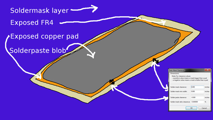
Since I hadn't done a stencil before, there was a bit of a learning curve. I found some resources that helped me get started. The first was this page from rheingold heavy which introduced some of the parameters needed, such as the solder paste clearance, to get the gerber files ready to send to oshstencil. The second resource was from this forum post on the kicad.info forums. Specifically this picture helped me visualize how the pad mask parameters in Kicad worked :
The first step for me was to determine which pads on the PCB required a stencil. At first I was thinking about just including all the SMD components. But after giving it some more thought I opted to leave out the SMA connector and shield, since I wanted to be able to test the circuit out first before sealing it in its metal house. And the SMA connector would require some hand soldering to get a good connection.
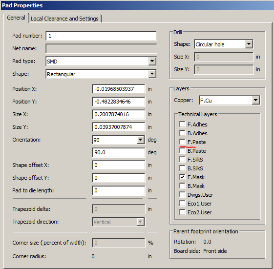
Now that I knew which SMD pads I wanted to exclude from the stencil, I took those pads out of the stencil by unchecking the F. Paste layer (the front solder paste layer) from the Technical Layers area of the Footprint Editor. This disassociates the pad from the front solder paste layer. It looks like F. Paste is checked by default whenever you create a new SMD pad.
The next thing I learned was that there should be a little bit of clearance between the solder paste and the edge of the pad. This clearance is aptly named "Solder Paste Clearance" and is illustrated on the picture above. This property can be adjusted on a per pad level on the pad properties page, or on a global level. To set the clearance for the entire PCB you navigate to Dimensions -> Pads Mask Clearance from the Pcbnew screen.
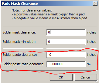
On the Pads Mask Clearance screen, there are 2 options for adjusting the solder paste clearance. You can either choose to set the clearance a fixed amount from the edge of the pad, or you can set the clearance to be a ratio based on the size of the pad. I chose to give the clearance a ratio of -5%. After adjusting these properties, the only thing left to do was to generate the gerber files which will be sent to oshstencils. When you go to generate the gerbers, you only need to select the solder paste layer as well as the edge cuts layer, since those are the layers that oshstencils care about.
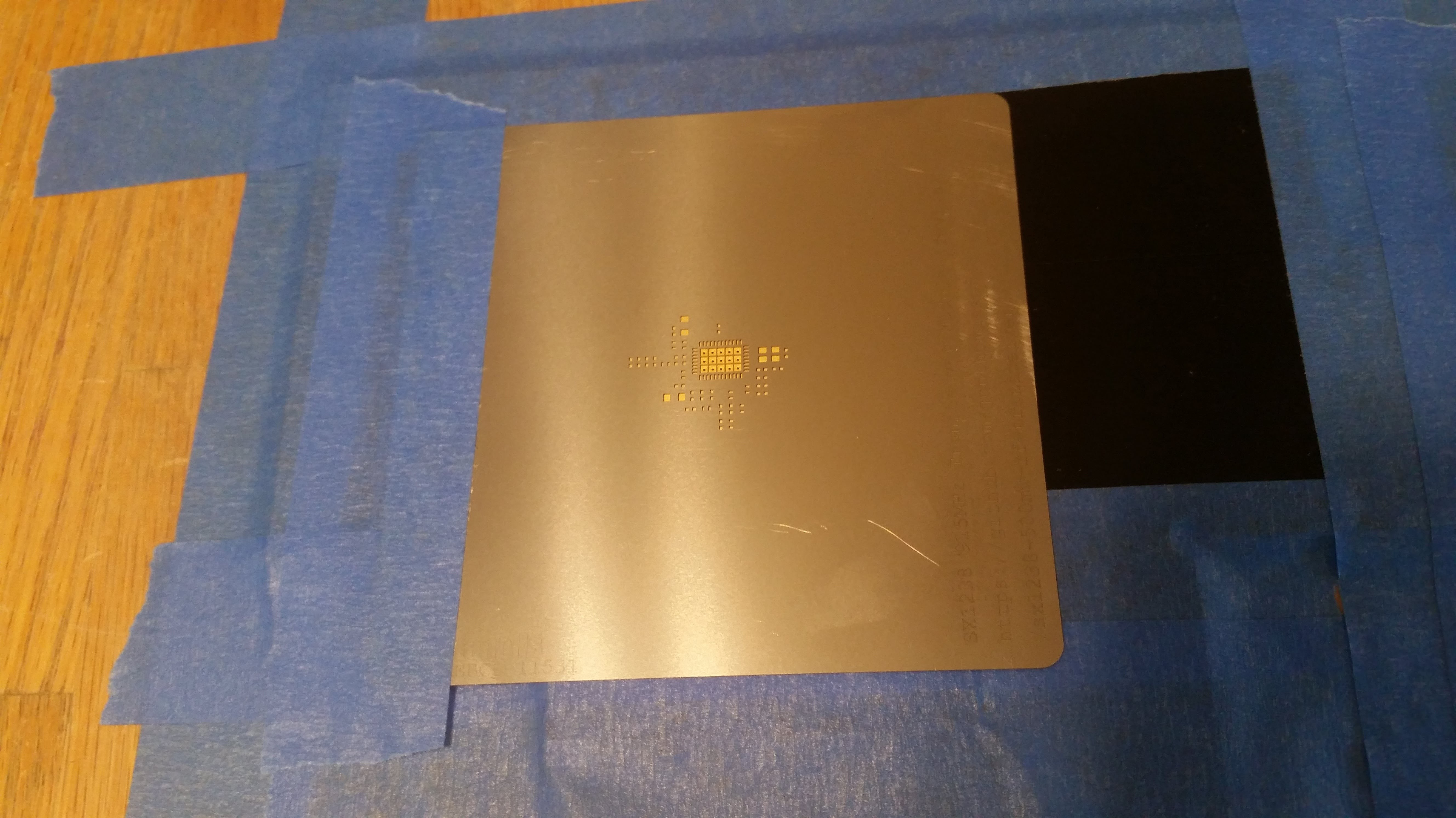
I was surprised at how quickly I received the stencil back. It seemed like it only took 2-3 days from the time of order to having the stencil in my hand! Besides the stencil, I also ordered a little jig to hold the stencil in position while applying the paste. I found out you can also just use unpopulated PCB’s to fashion your own jig. Here’s a pic of what I came up with:
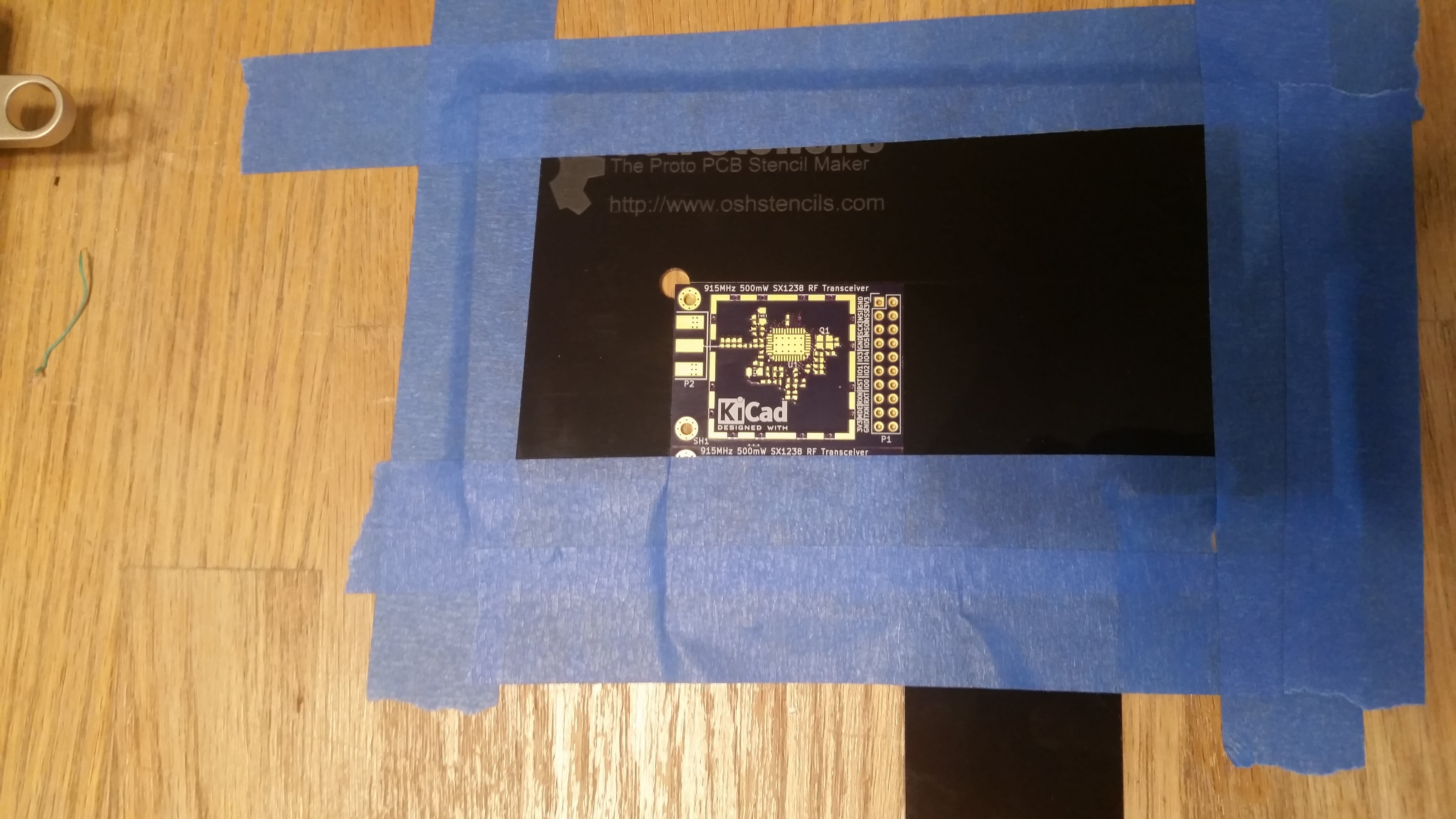
Once the jig and PCB are in place, you lay the stencil over the PCB until all the pads match up and are visible through the appropriate cutouts of the stencil. Then you tape the stencil down on one side.
From here, my pictures were a little too blurry to share, but I basically followed the same procedure for applying the paste presented in this Sparkfun video. The important thing I learned from all of this was to make sure to clean up the solder paste from the stencil and anything else you want to keep right away. Otherwise it really gets tough to clean up, and it manages to get everywhere!
To reflow the solder paste after I had placed the components I simply used a hot air rework gun. I did have some solder bridges around one of the transceiver chips, but nothing a little drag soldering couldn’t fix. Here’s the finished boards (with a quarter for size reference):

Discussions
Become a Hackaday.io Member
Create an account to leave a comment. Already have an account? Log In.