 avishorp
Circuit Design
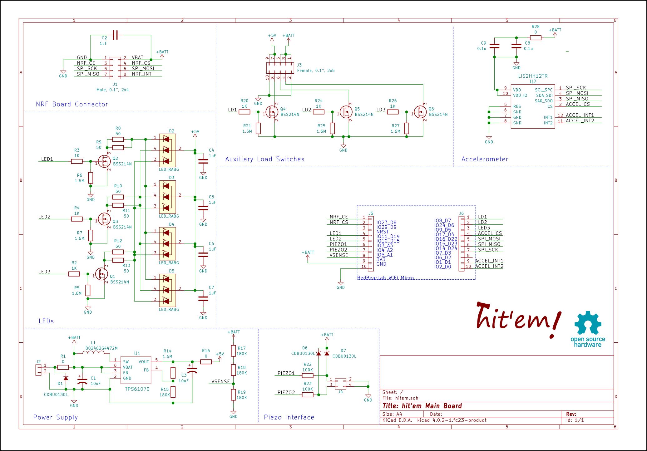
As mentioned in a previous post, the circuit board is designed to be shared between the hammer and the hat, thereby reducing the design effort.
The main component is, of course, the WiFi Micro module. It does all the heavy lifting of processing and communication. The module is connected to the main board using two single row, .100" spaced header connectors. Beside the module there are drivers for the RGB LEDs (there are four LEDs mounted at the corners of the board), a power supply circuit and an accelerometer.
The circuit is designed to be powered by a pair of AAA batteries. This gives us a nominal operating voltage of 3.2V - 2.4V. Luckily, the CC3200 chip on the WiFi Micro module is designed exactly to work in such a voltage range, so it is connected directly to the battery power input. The problem arises with the LEDs. Some of them have very high Vf, approaching 3V, making them hard to drive directly from a 2xAAA setup. Therefore, I included a step up booster on the board, based on TI ???????. This chip is completely integrated with the power switch, it only needs an inductor and couple of capacitors.
The accelerometer, ?????, is also quite simple, also capable of being directly powered by a pair of AAA batteries and connecting to the WiFi module via an SPI bus. I did include a jumper resistor, for disconnecting it from power completely, since I was not sure I would be able to assemble it. The power supply also has jumpers in the input and in the output, to ease testing and debugging.
PCB Design
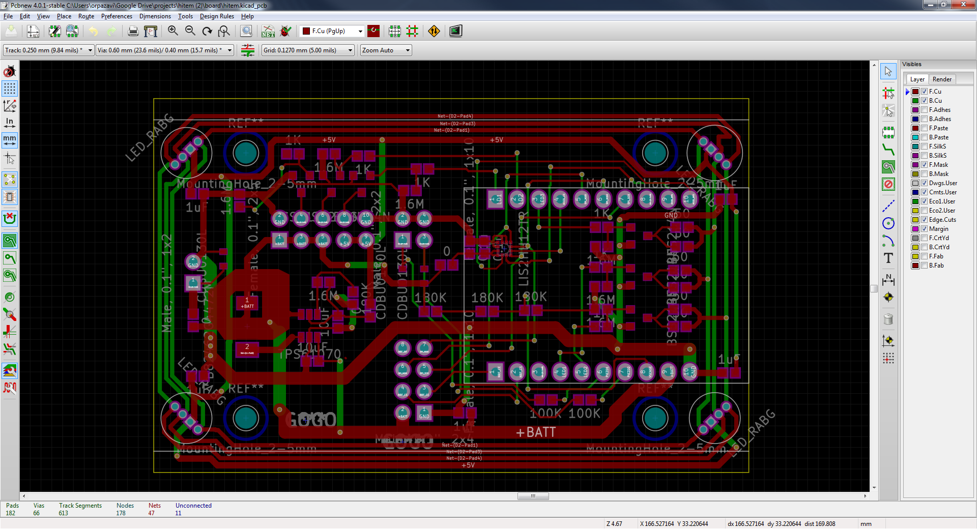
The PCB design is pretty straight forward. It's size is 70x40mm, making it cheap to fabricate in common 100x100mm slice offered by Chinese manufacturers. The WiFI Micro connectors are on one of the short edges of the board and the four LEDs are mounted in the four corners. I opted for TH LEDs, because I had to mount them on both sides of the board, and that is hard to achieve in home reflow process (in retrospective, that was not a wise decision; soldering those LEDs manually consumed a lot of time).
The PCB is relatively sparse and there were no notable routing or placement challenges.
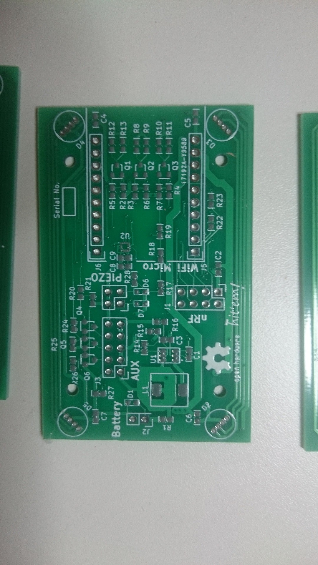
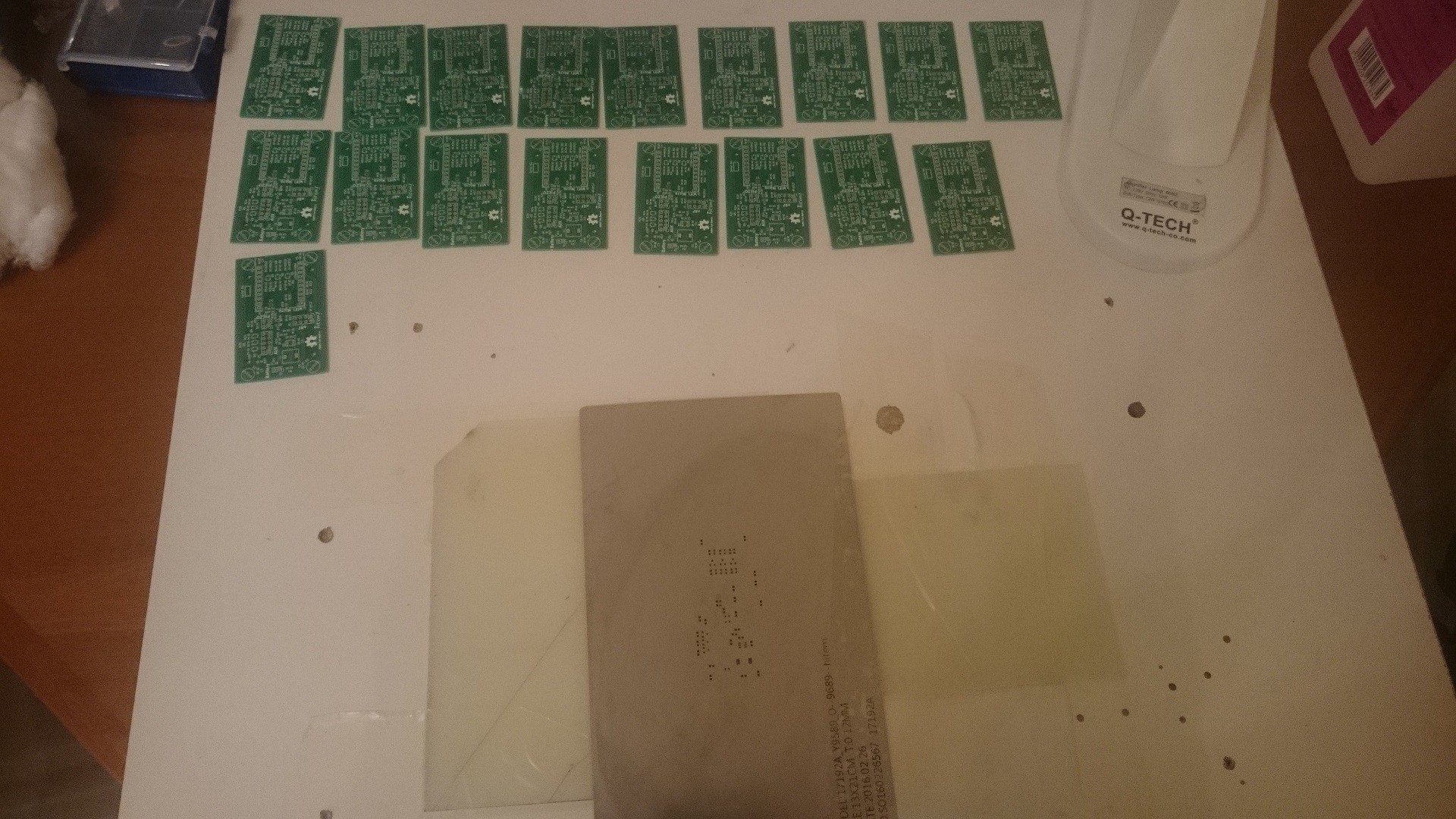
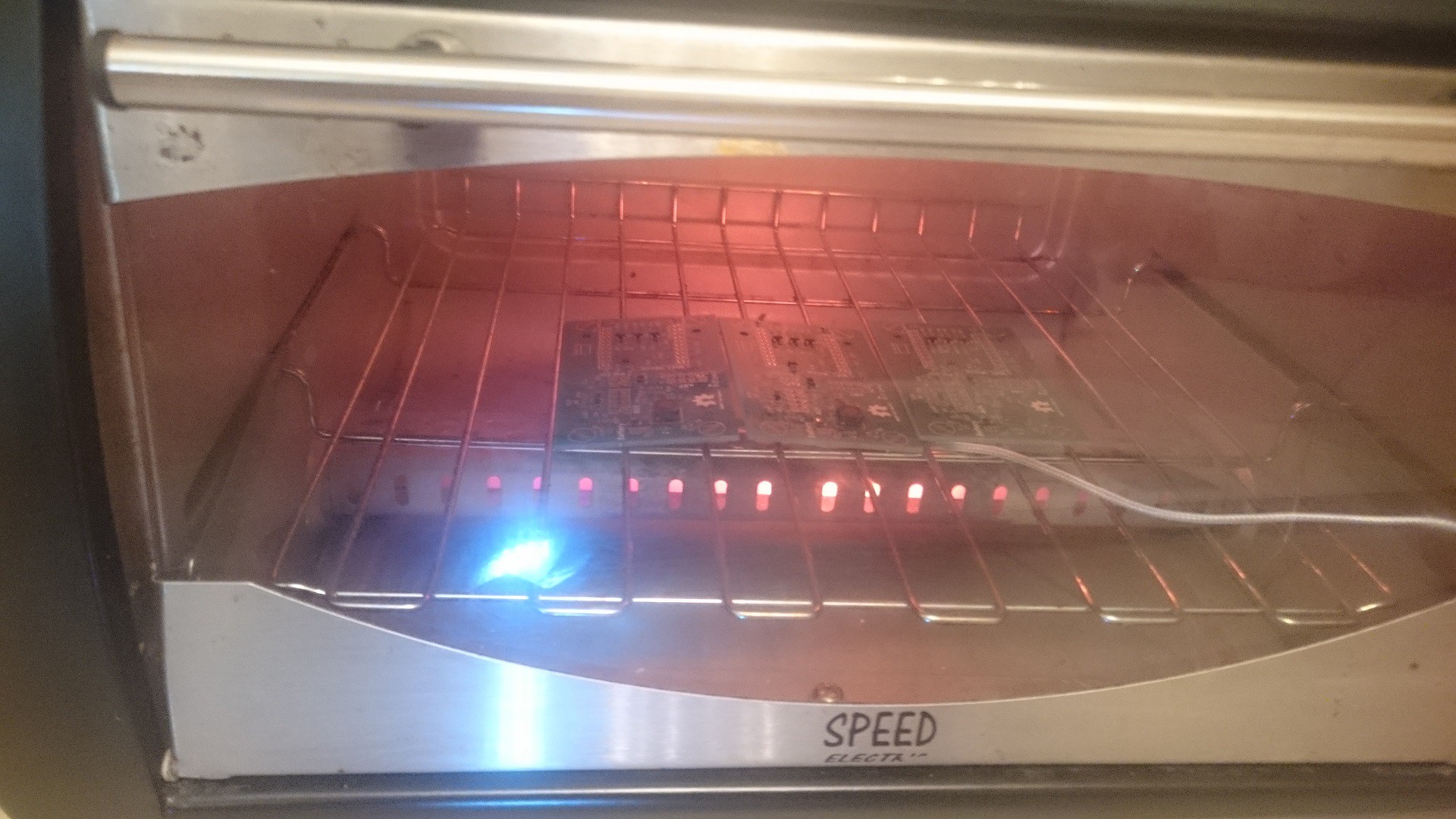
Assembly
Having to assemble ~20 boards, reflow soldering was a natural choice. This is the first time I was doing such a procedure, and overall, it went pretty well.
The one exception was the soldering of the tiny accelerometer. As I anticipated, it was pretty hard. It started with the application of the solder paste which smeared around the tiny pads, the placement of the component without a proper microscope and finally - checking whether the soldering was successful. After a few failed attempts, I understood that It's not going to work the tight schedule and decided to give up on the trials and back off the the backup plan - using piezo sensors for hit detection.
Discussions
Become a Hackaday.io Member
Create an account to leave a comment. Already have an account? Log In.