 Sankalp Modi
This log talks on how to assemble the internal circuits of Open Indirect Ophthalmoscope.
Dismantling:
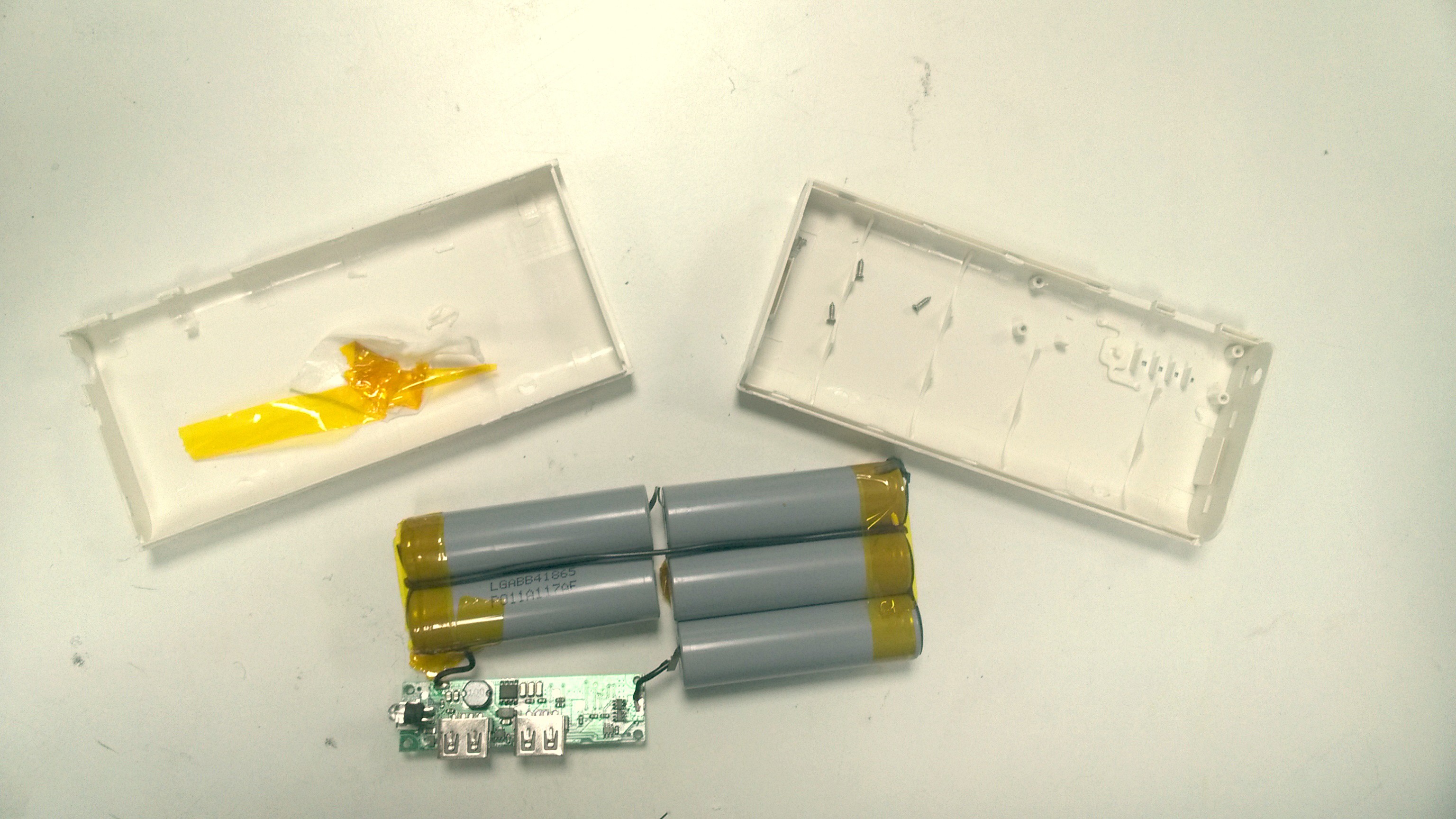
Crack open the power bank (13,000 mAh power bank with power output of DC 5V, a device with two output USB ports such that one gives a current of 2.1 Amps and the other 1 Amp.)
The reason for choosing a power bank with two such outputs is that the LED circuit and the RasPi together need a higher current, which in this case is being powered by the 2.1 Amp port and the display is powered by the 1 Amp port.
While doing this, care should be taken that the circuit is not damaged. Power cables are soldered onto the PCB, therefore after cracking, do not jerk open the bank.
Here are some references for the power banks that can be used.
http://amzn.to/2cNw0av
http://amzn.to/2d4wjNt
It is preferable to use a power bank with the USB A Type and Power Bank Charger - USB B Type on adjacent sides. This makes the assembly easier.
Remove the batteries carefully from the casing. There should be five batteries, remove one battery out from the circuit by cutting the metal plate interconnecting the batteries.
Once this has been done, separate out the batteries into sets of two with both sets electrically parallel to each other. At this point connect two sets of wires connecting two sets of batteries, while doing so place the heat shrink material in the wire, this will be used to make the wires appear seamless and give them strength once all the connections have been soldered.
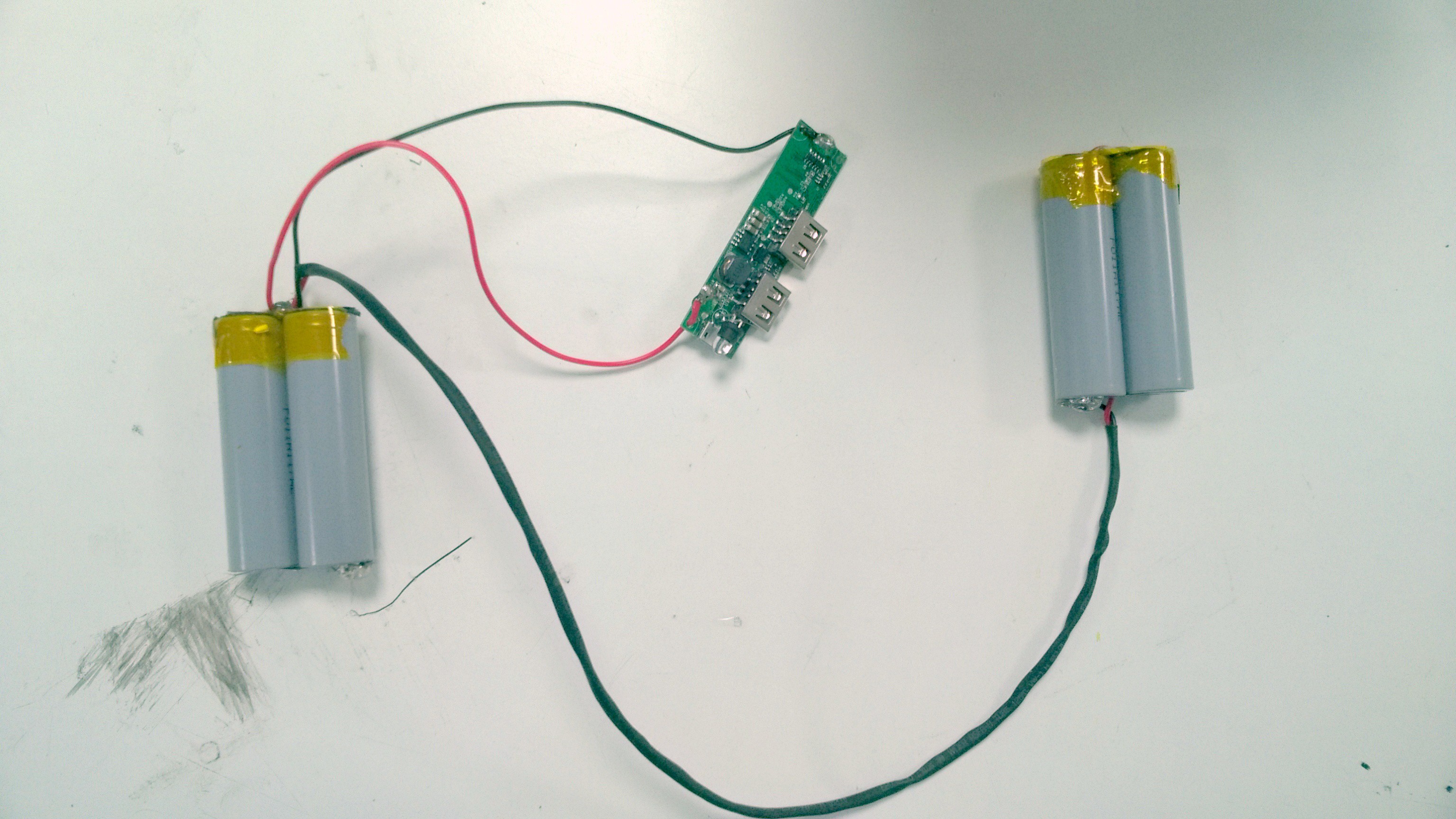
The separation of batteries is done so as to provide an even weight distribution throughout the chassis. Placing two sets of two batteries each makes the weight balance out horizontally.
These wires should be placed such that the ones connecting the positive ends are slightly longer than the negative ones. Carefully pass the positive wire in the crevice between the batteries. Solder the negative terminals. The resultant battery setup should look like this:
This allows the batteries and the wires to seamlessly fit in the battery encapsulation groove in the 3D printed assembly. Carefully place the batteries and check the wire lengths.
Now take the PCB from the power bank and increase the length of the wires connecting the batteries to the PCB. They should be connected onto a terminal 'B+' for the positive terminal and 'B-' for the negative terminal respectively. Solder the terminals and seal the solder with silicone glue to give the entire joint some strength.
On the same PCB extract the USB ports by heating their soldered ends (4 Connections) from one side using a hot air blow gun or a solder gun and pulling from the other end simultaneously. Be careful to not pull too hard, as this might cause the circuit to get damaged.
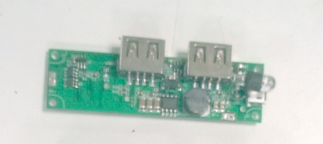
After the USBs have been extracted, it's time to solder the cables connecting the power supplies to the PCB and the LCD.
Take a micro USB cable and cut off the non micro USB end. Strip this end and peel the wires out. There should be two wires (if you are using a charging cable) or four wires (if you are using a charging & data transfer cable). The standard colour combination is Red - for the positive connection and Black - for the negative connection. Solder the red wire to the positive end and black to the negative/ground on the power bank PCB at the 1 Ampere port. This cable will supply power to the custom LCD.
Take another set of two wires (red & black preferably) and solder the red end to positive and black end to negative/ground of the Power Bank PCB's 2.1 Ampere port. Take the other end of the wire and attach two female headers on to it. These will be connected to the custom PCB's power supply. This will be used to supply the power to the LEDs illuminating the retina and to the Raspberry Pi.
Soldering the Ras-Pi Shield PCB
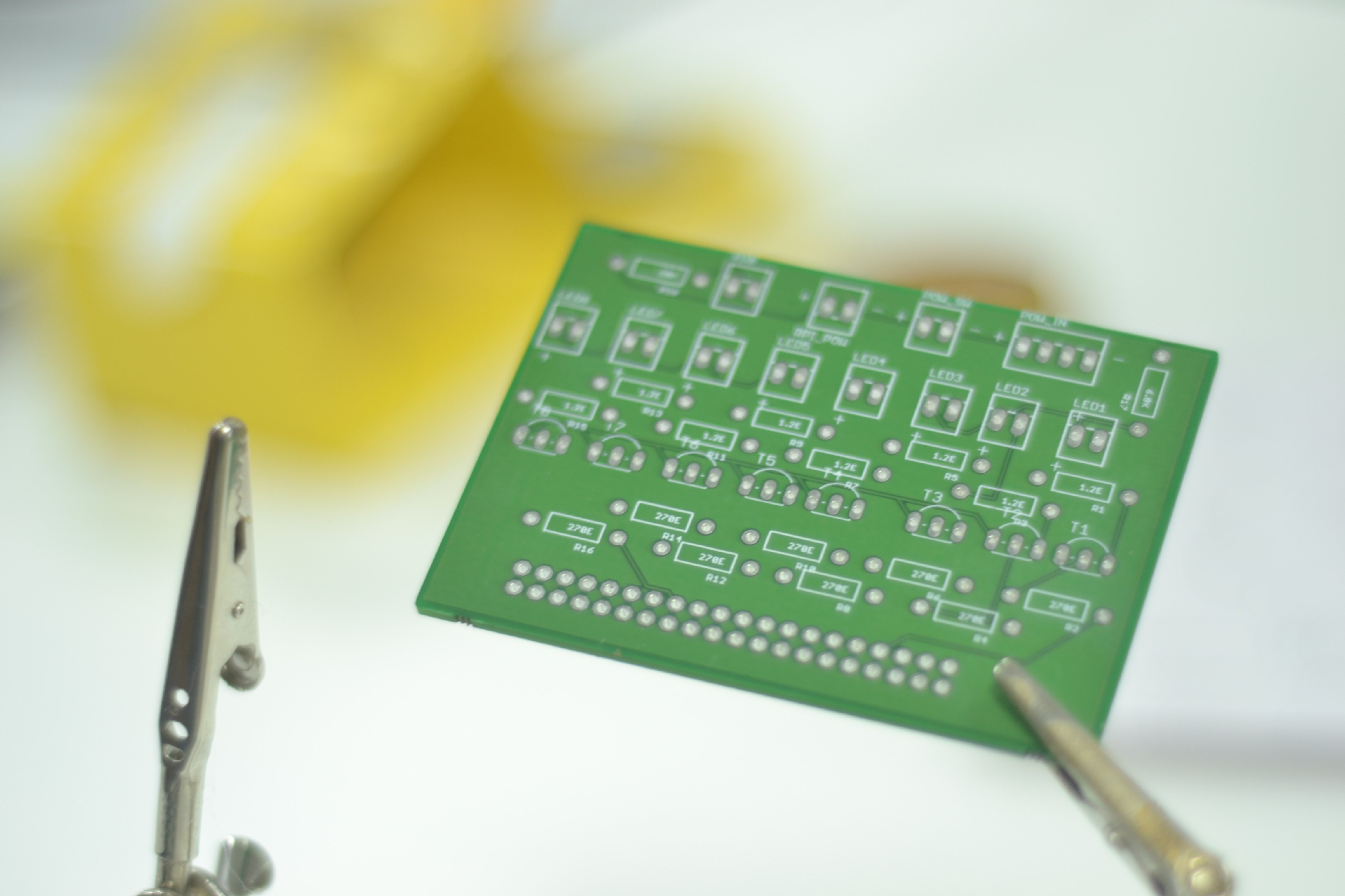
Place the 2N222 Bipolar Junction Transistors (BJTs) carefully on the PCB. Most PCBs come with a hemispherical marking and a flat end marking to ensure correct orientation. Though this may not be true in all cases, in such a situation one way to understand the placement is to place the transistor such that the flat side if facing you and the pins are pointing upwards, in the orientation the pins are in the order - Emitter-Base-Collector from left to right (clockwise order). The connections of emitter base and collector are as follows with standard notations applicable.

For any other clarifications please refer to the Schematic and Gerber files.
Place the female headers on the rail that falls directly on to the Raspberry Pi GPIO Pins. Remember the pins of the RasPi are male headers. Once this is done, solder each node separately and carefully. Ensure that there is no extra solder blob.
Now carefully take 8 resistors each of 270 Ohms (Colour Code: Red | Violet | Brown | Gold) and place them below the transistor on the ports marked as | 270E |. Solder each carefully and cut off the extra metal from the terminal.
Again take 8 resistors each of 12 Ohms ( Colour Code: Brown | Red | Black | Gold ) and place them at the ports above the transistors, marked as | 1.2E |. Solder each carefully and cut off the extra metal from the terminal.
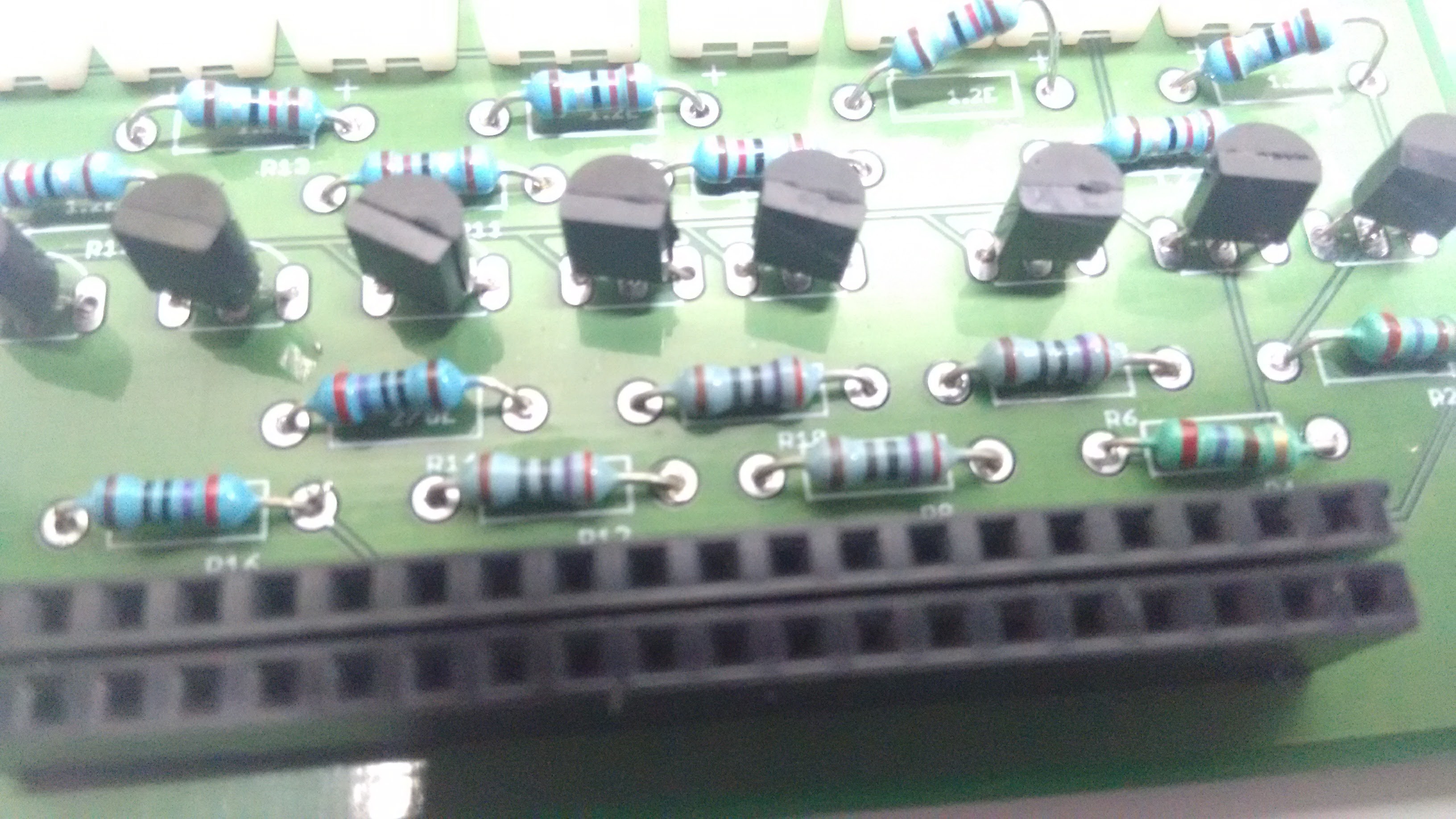
Take a 6.8K Ohm ( Blue | Grey | Red | Gold ) resistor and place on the top left slot for it labelled as R17. Solder and remove extra ends from the terminals.
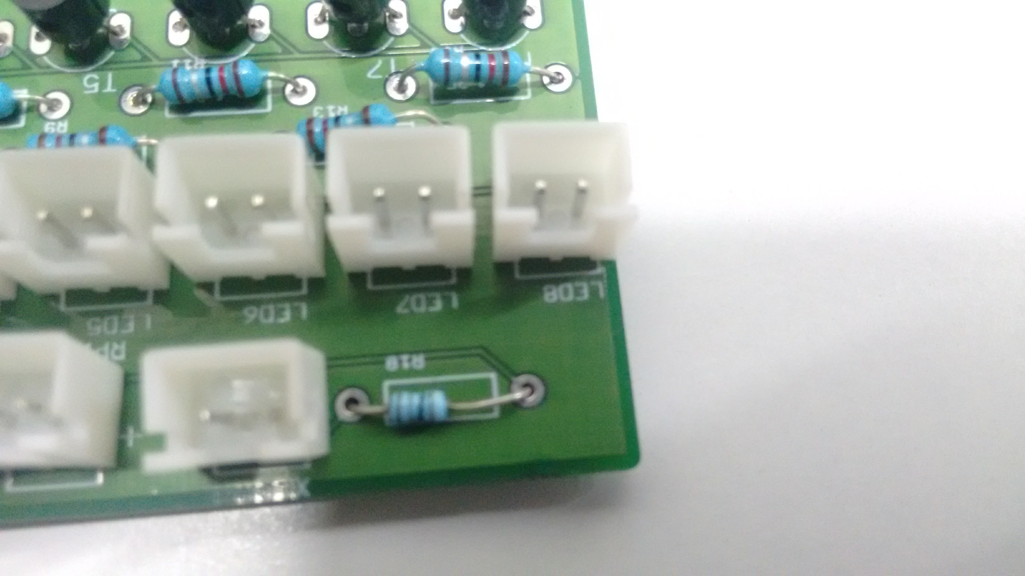
 Now take 11 two-pin male headers and place them on the top of the PCB. Solder them carefully form the other side of the PCB.
Take a 4-pin male header and place it on the power port on the top right of the PCB, adjacent to the 6.8 K Ohm resistor and solder carefully.
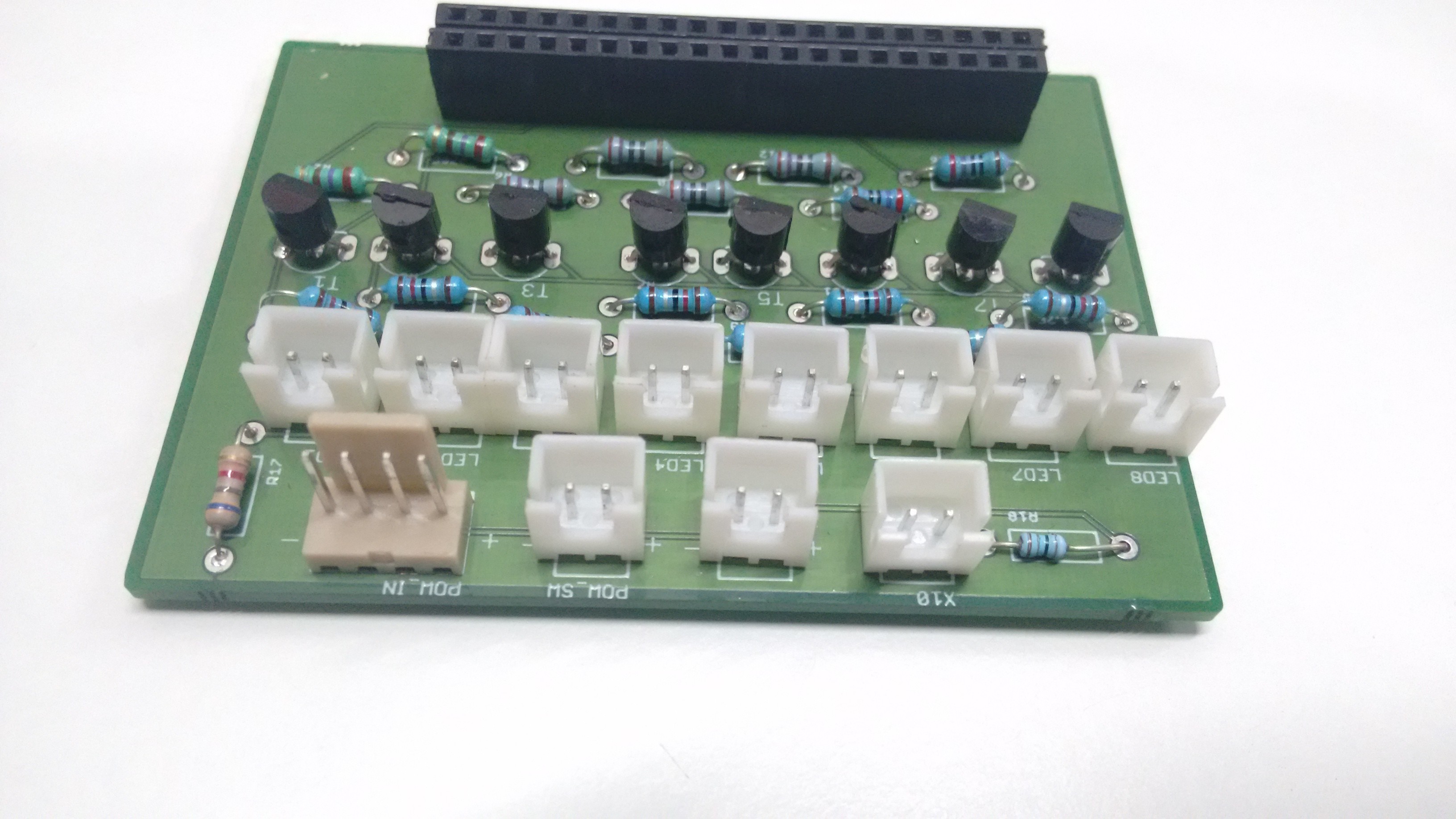
The PCB should look like this once everything has been soldered.
Discussions
Become a Hackaday.io Member
Create an account to leave a comment. Already have an account? Log In.