 Jeremy
Full Disclosure: I have to give credit where credit is due. Everything I learned about home etching was from this HackADay article. I fully recommend you read it, and tailor the etching methods to your equipment and materials.
http://hackaday.com/2008/07/28/how-to-etch-a-single-sided-pcb/
PCB Etching is an art. You need the correct paper, apply right amount of pressure, create an acid bath, and have tons of patience. It took me around a dozen attempts in order to perfect the process for my environment, so by the time it came to create the FlightCPU, it only took 3 boars (1 wasted). Below is a visual walkthrough to help identify the steps it takes to home etch a PCB.
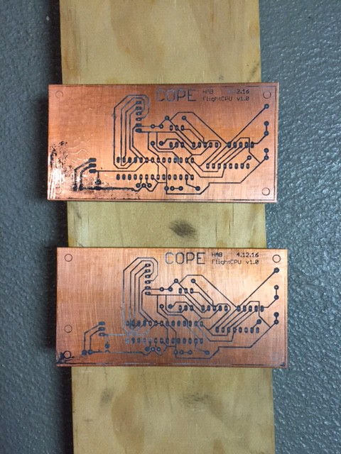
In true Contact fashion.. why build one when you can build two for twice the price.
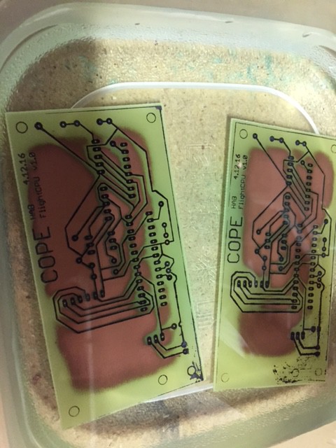
The acid bath etches away the copper on the board, leaving only the traces applied during the ink transfer process. Here you can see the acid doing its part, eroding from the edges to the middle. I find it is best to wipe the board with a brush as it etches to help evenly distribute the acid bath.
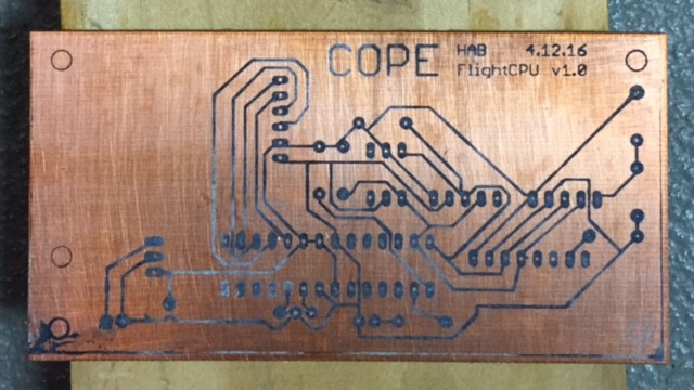
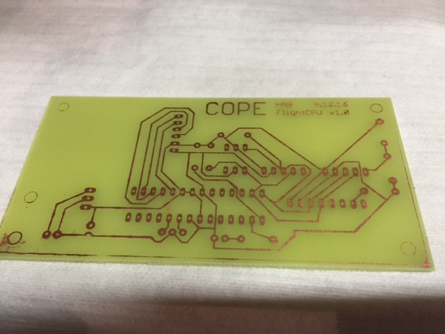
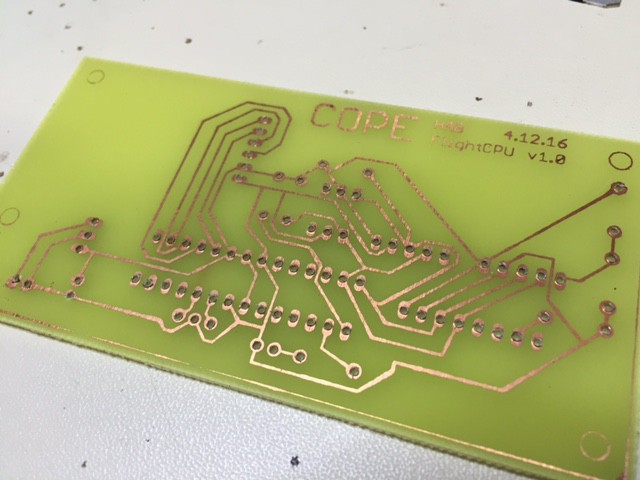
Here you can see the final product before we head over the the drill press and create holes for all the components. I used paint thiner to clean off the ink from the traces, exposing the copper lines that will be the electrical traces for the components. Not a bad job!
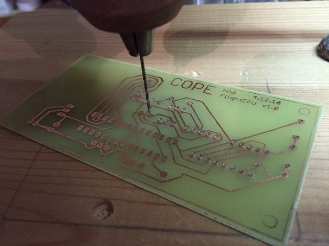
A drill press is a must if you are serious about creating your own PCBs at home. There is no other way to ensure straight perpendicular holes when drilling into PCB. Also, the copper helps guide the drill bit into the correct place, so once you get into a groove, everything just comes together.
And finally, the finished product. Well, the PCB at least. We still have to assemble the components and solder every junction, but that might have to wait for another log update.
Discussions
Become a Hackaday.io Member
Create an account to leave a comment. Already have an account? Log In.